Digital Tension Scale

Posted 27 October 2018

I recently underwent rotator cuff repair surgery on my left (dominant) shoulder, and am now starting the rehab process.   My PT person was adamant that I not re-start my normal rowing routine for at least six weeks post-op, due to the possibility that I could re-tear the tendon.   This made me curious as to what the tension really was on my arms when rowing, so I decided to try and build a digital dynamic tension sensor, capable of plotting rowing strap tension in real time.

To start, I had to educate myself on the world of strain gauges and load cells, and what the differences are.   As I came to understand, what I wanted was a  load cell configured for tension measurement, with a  strain gauge as the active sensing element in the load cell.   So, I started searching for load cells, and was immediately inundated with ‘too much information’.   This deluge is certainly better than the old days where I had to search through paper (really, no internet!) magazines and catalogs, but at least you didn’t have to worry about overload headaches! ;-).

Anyway, I found this item ‘Degraw 40Kg Tension Load Cell and HX711 Combo Pack Kit‘, as shown in the screenshot below

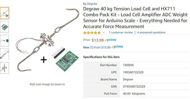
Amazon catalog item for Degraw load cell

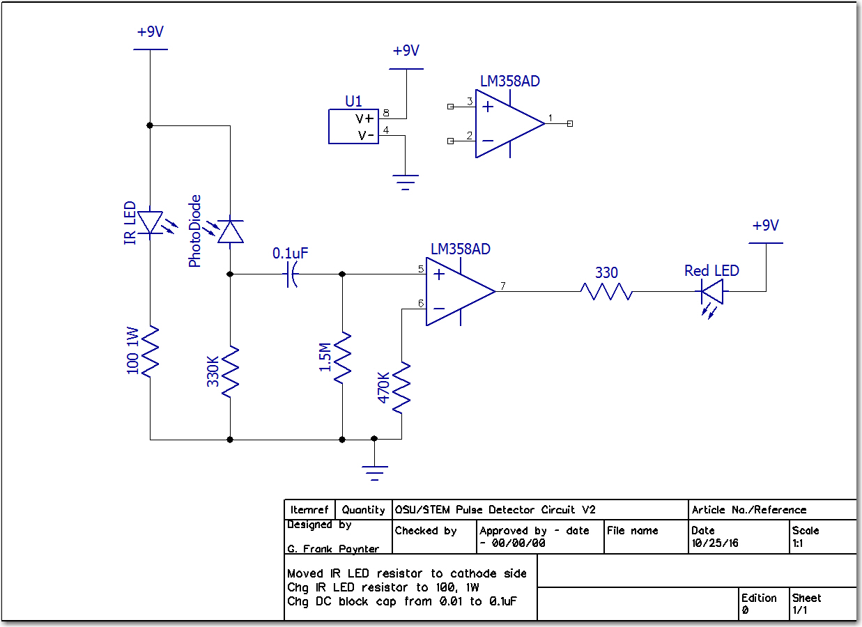
This looked perfect for my intended use, as I could hook one end onto my rowing machine strap, and connect some sort of handle to the other end.   Now all I had to do was figure out how to hook the thing up and get it to work.   Fortunately Degraw also provided a sketch of the hookup using an Arduino Uno, so that part was pretty easy.

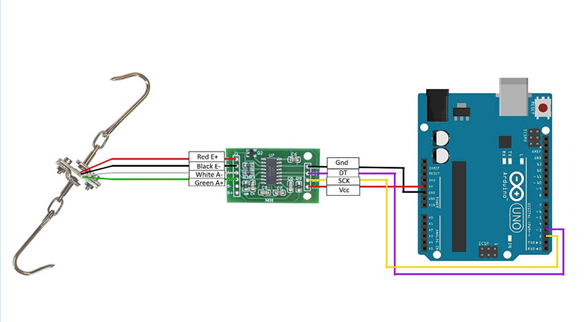
Degraw-provided hookup diagram

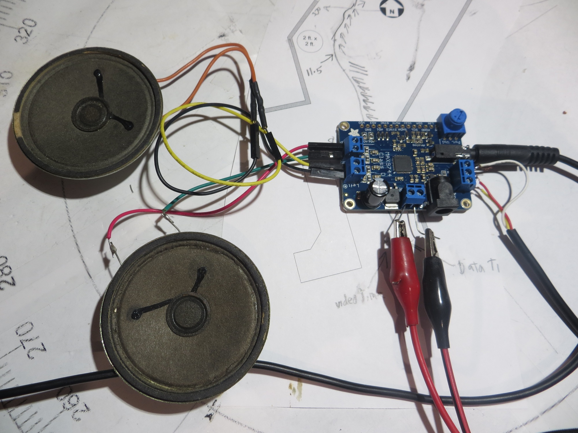
After a bit more research, I found a nice HX711 library by bogde and some example programs, and got the whole thing to work using an Arduino Mega 2560.   Once I got a program running with some preliminary (but believable) results, I started thinking about how I was going to manage the physical aspects of hooking this assemblage to the rowing machine and recording dynamic tension.   I couldn’t really just let the HX711 board hang by the strain gauge wires while connected with jumpers to the Mega board, as the #28 strain gauge leads would surely break.   So, I came up with the idea of somehow attaching the HX711 board and a small microcontroller to the load cell assembly, and then connecting the whole thing to my laptop with a USB cable.   Hopefully the USB cable would be long enough to allow full extension of the rowing machine strap so I could collect full rowing cycle data.

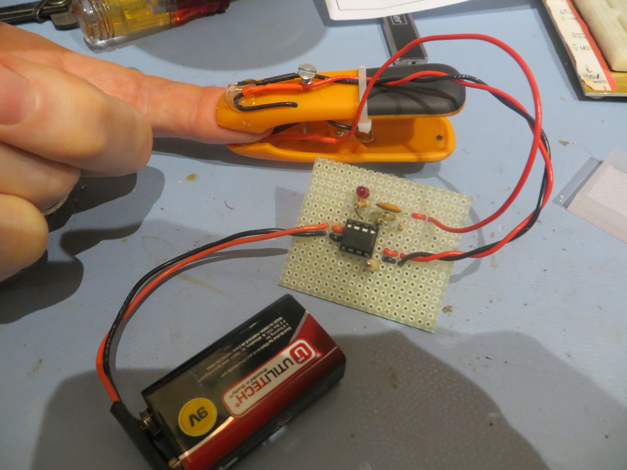
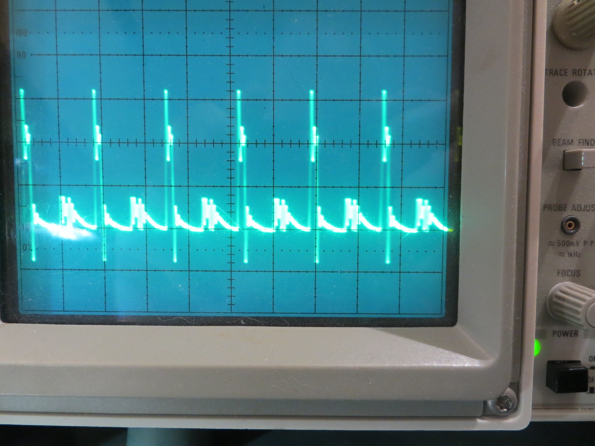
After some digging around in my parts cabinets, I came up with two candidates for the ‘small microcontroller’ part of the plan; a 3.3V Teensy 3.2, and a 5V/16MHz Sparkfun Pro Micro.   I tried the Pro Micro at first, and almost immediately went down the rabbit hole (my term for getting lost in some technical wonderland without a clue how to get back) trying to figure out how to program the device – a challenge due to the way it handles com ports through the USB connector (it actually implements two different ones, depending on whether the boot loader or the user firmware is running – yowie!).   After climbing my way out of the rabbit hole, I decided to try the Teensy 3.2 instead, as I familiar with it from several other projects.   With the Teensy, I got a test program running and started taking data with known weights attached to the load cell. The way I did this was to suspend a plastic bucket from the load cell, and poured water into the bucket one liter (1Kg) at a time while recording data.   This was successful because I got good data, but unsuccessful because the data didn’t make much sense, as shown in the plot below

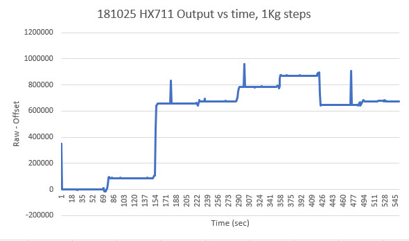
Results of pouring 1L (1Kg) water at a time into bucket suspended from load cell, using a 3.3VTeensy 3.2

As can be seen, the data was anything but the stairstep function I was expecting to see.   At this point I wasn’t sure if I had a hardware problem or a software problem, or something else entirely, so I sent an email to Degraw Product support with the above plot attached, asking if they had any insight into the problem.   Amazingly, they replied almost immediately, and offered to send me another load cell unit gratis so I could eliminate their hardware as the cause of the problem.   Although I was quite pleased with their offer of support, I thought maybe the 3.3V supply of the Teensy 3.2 might be causing the non-linearity (the HX711 advertises 2.7-5V operation but the lower voltage might be causing output linearity problems).   So, I tried again with the Sparkfun Pro Micro, and this time I managed to make the programming magic work. Then when I did the same test as above with the 5V Pro Micro instead of the 3.3V Teensy, I got the plot shown below.

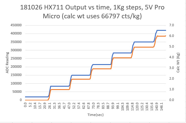
Tension vs time plot created by pouring 1L (1Kg) of water at a time into bucket suspended from load cell, using Sparkfun 5V Pro Micro

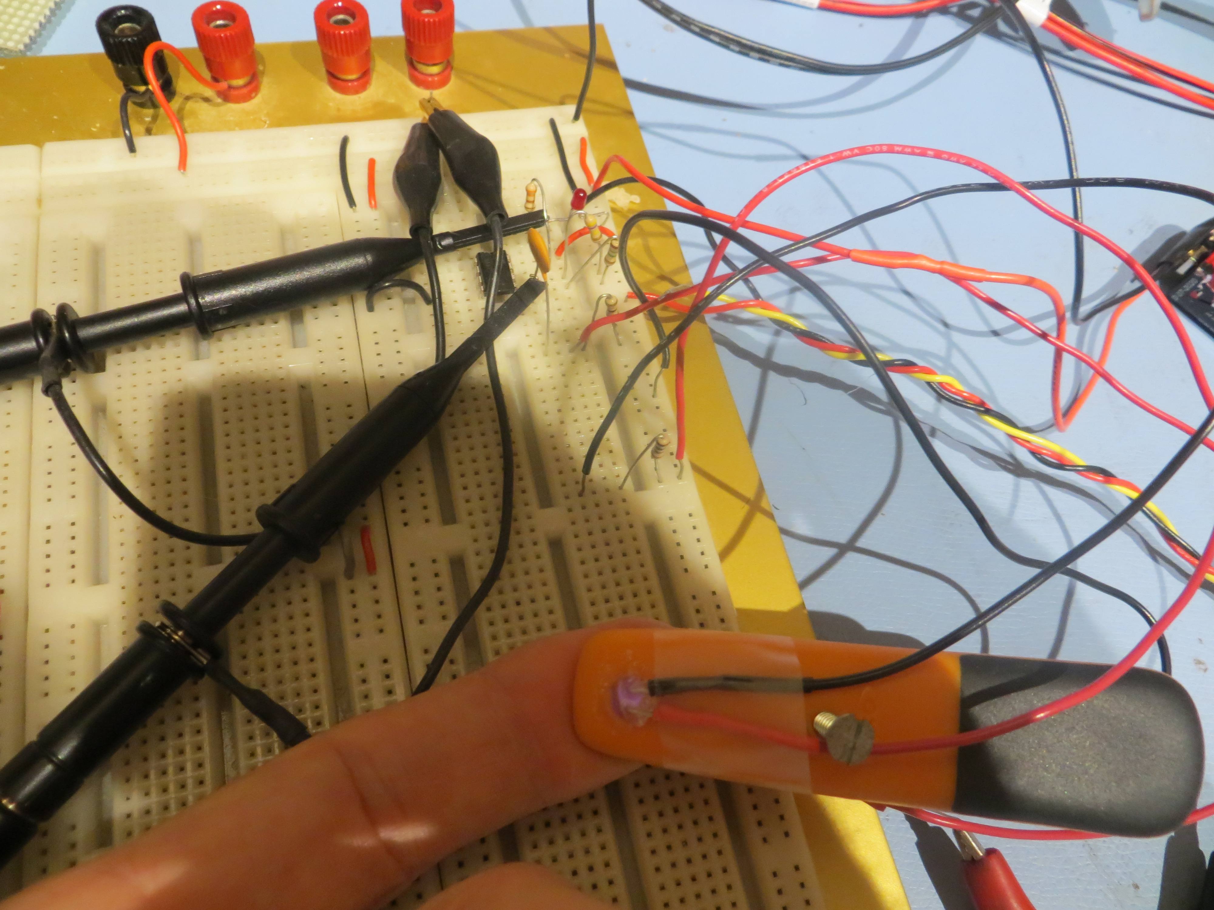
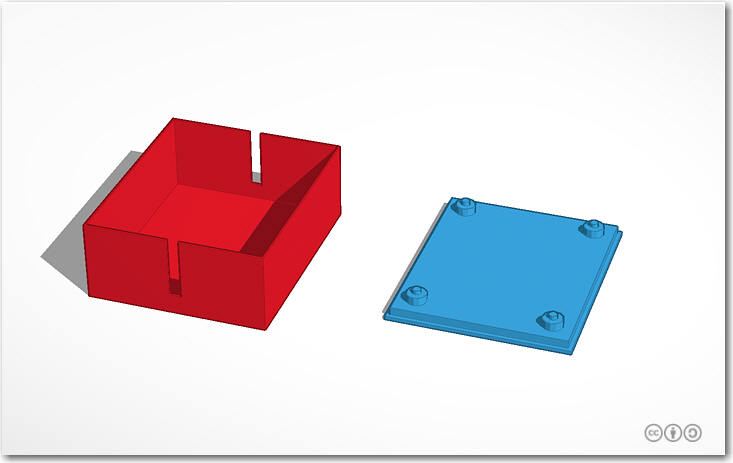
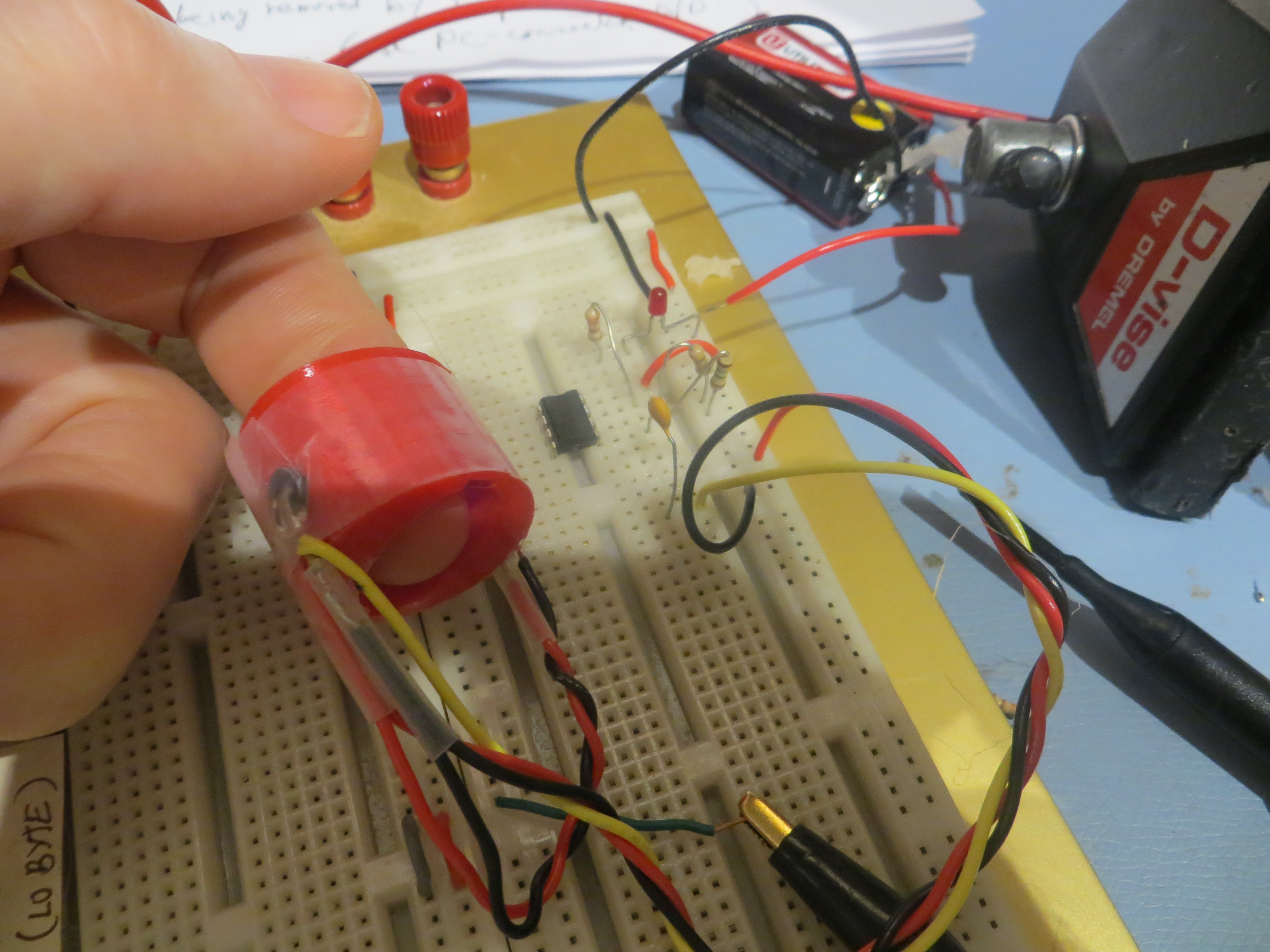
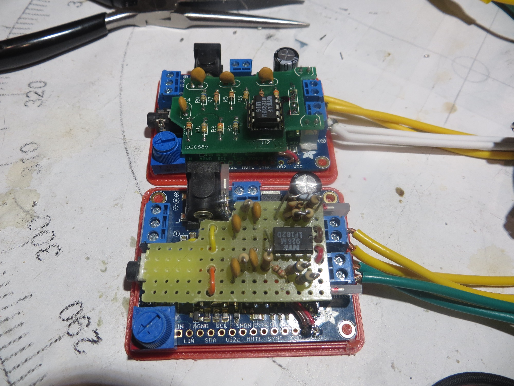
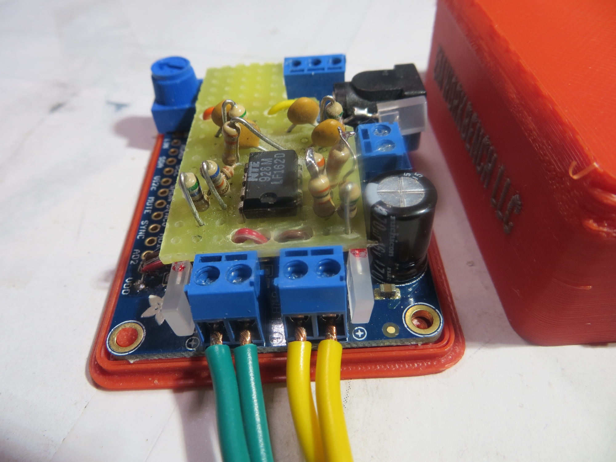
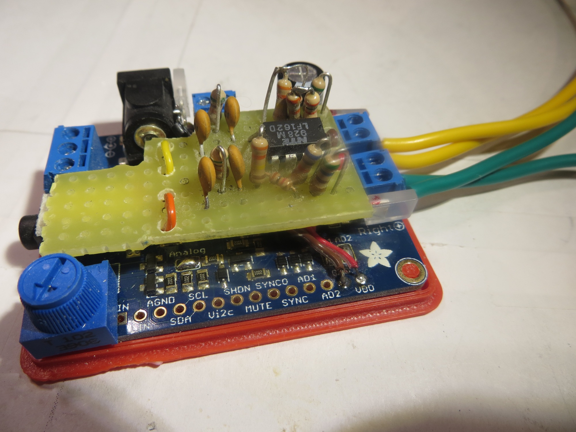
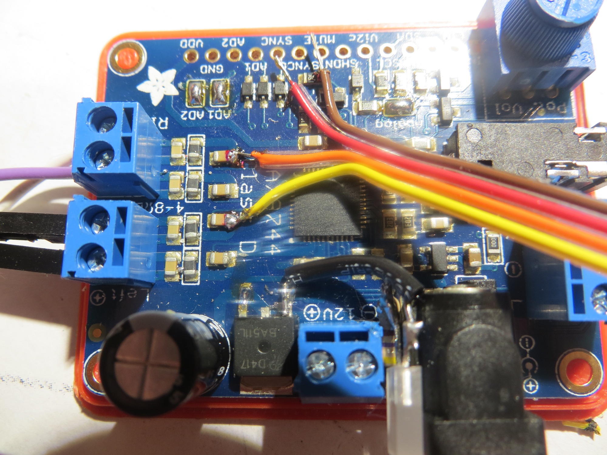
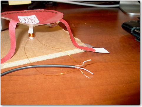
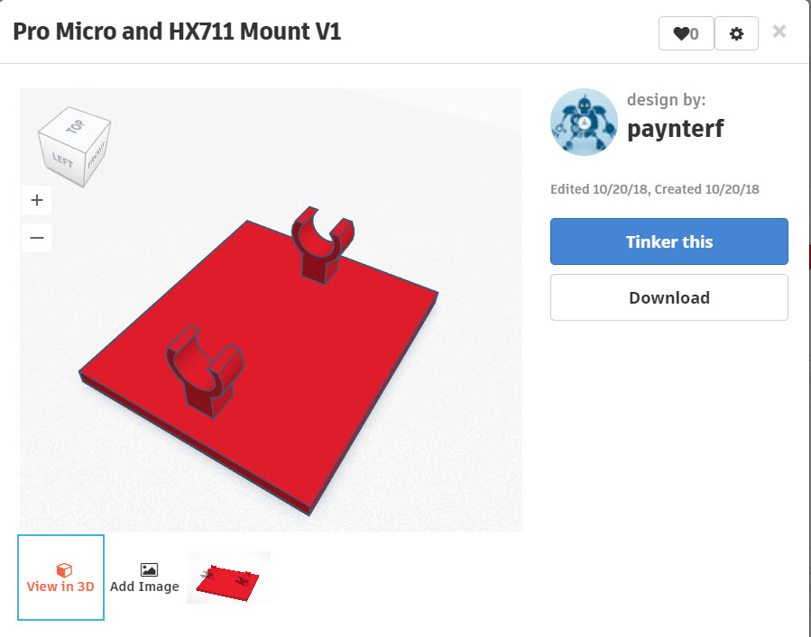
So, now that I had the software and microcontroller problems solved, I started working on the mounting issue.   After a few minutes in TinkerCad and some quality time with my PowerSpec 3D PRO 3D printer, I had a mounting platform that clipped onto the two vertical rods in the ‘S-shaped’ tension load cell, as shown in the images below.

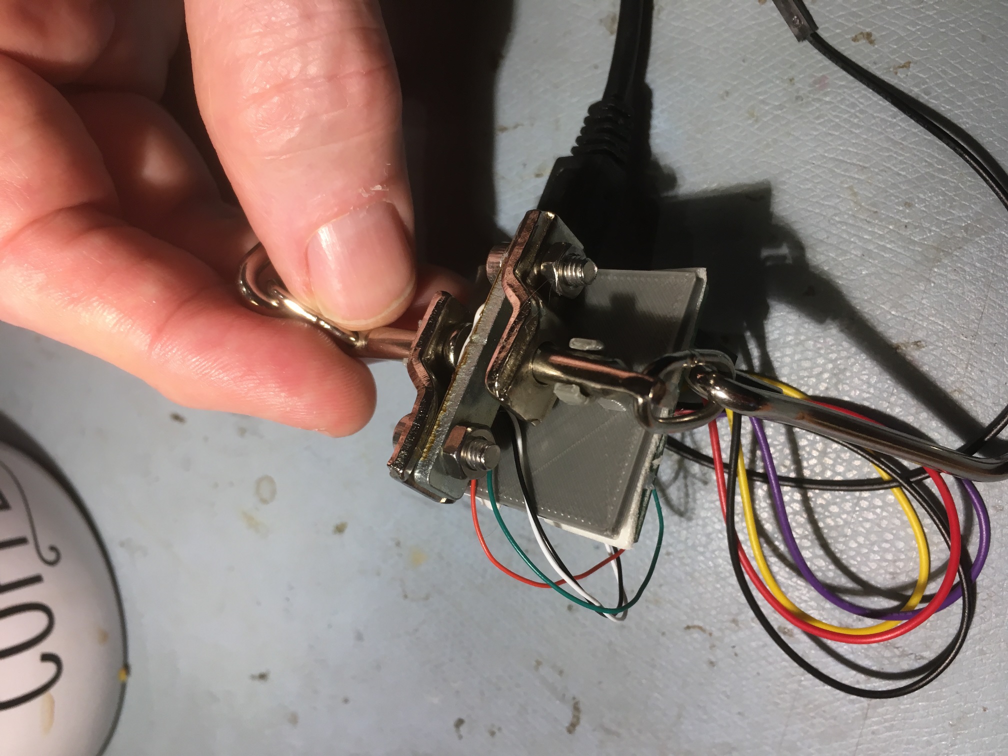
Reverse side of assembly, showing mounting plate clips attached to load cell vertical members

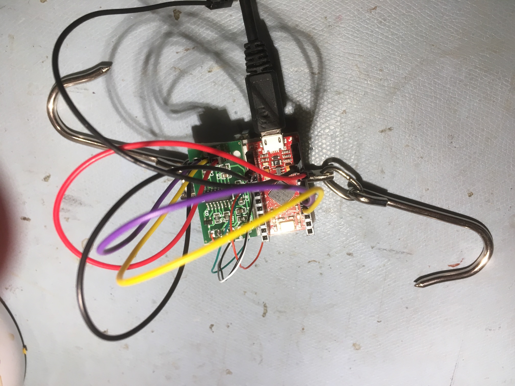
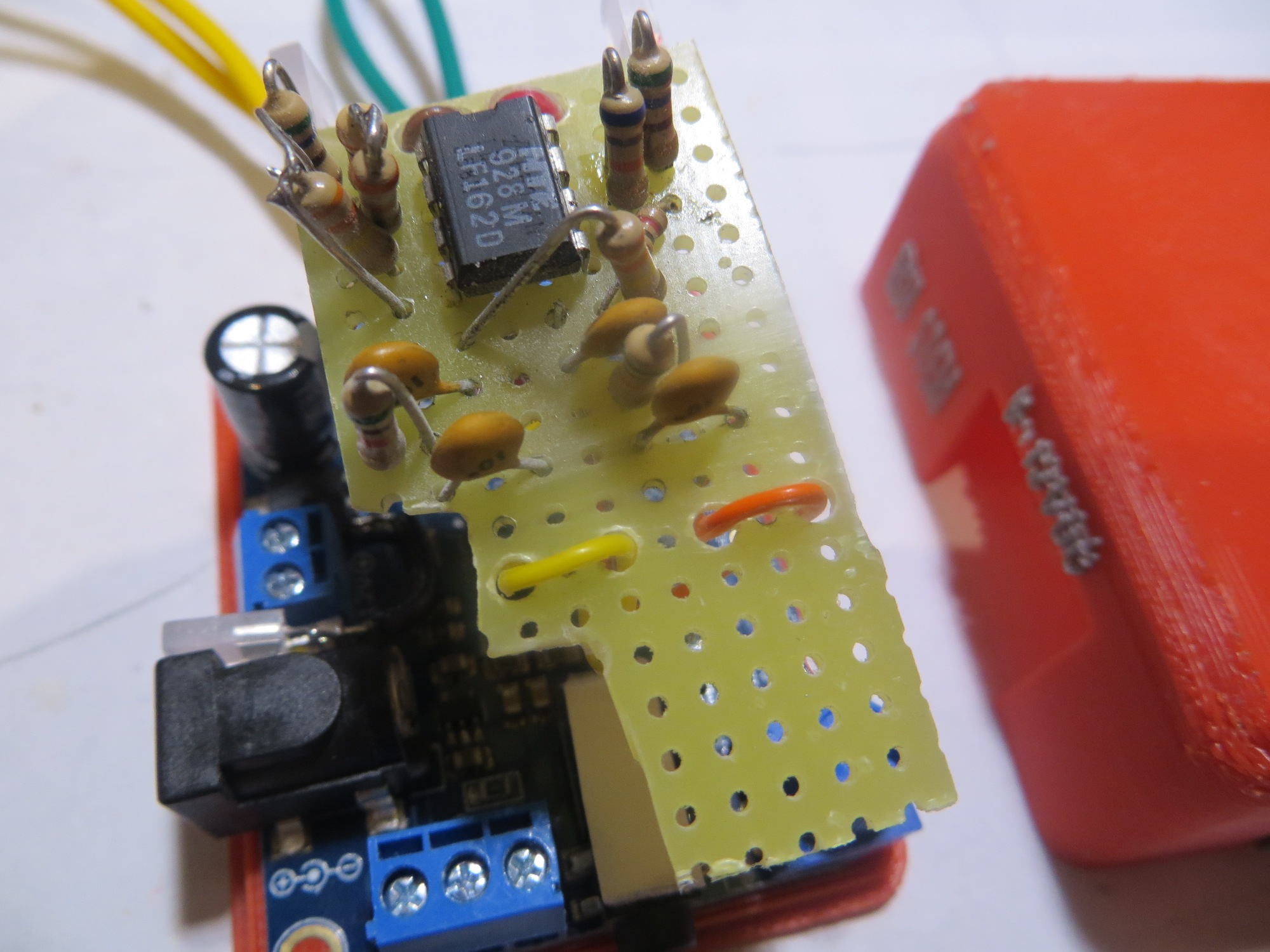
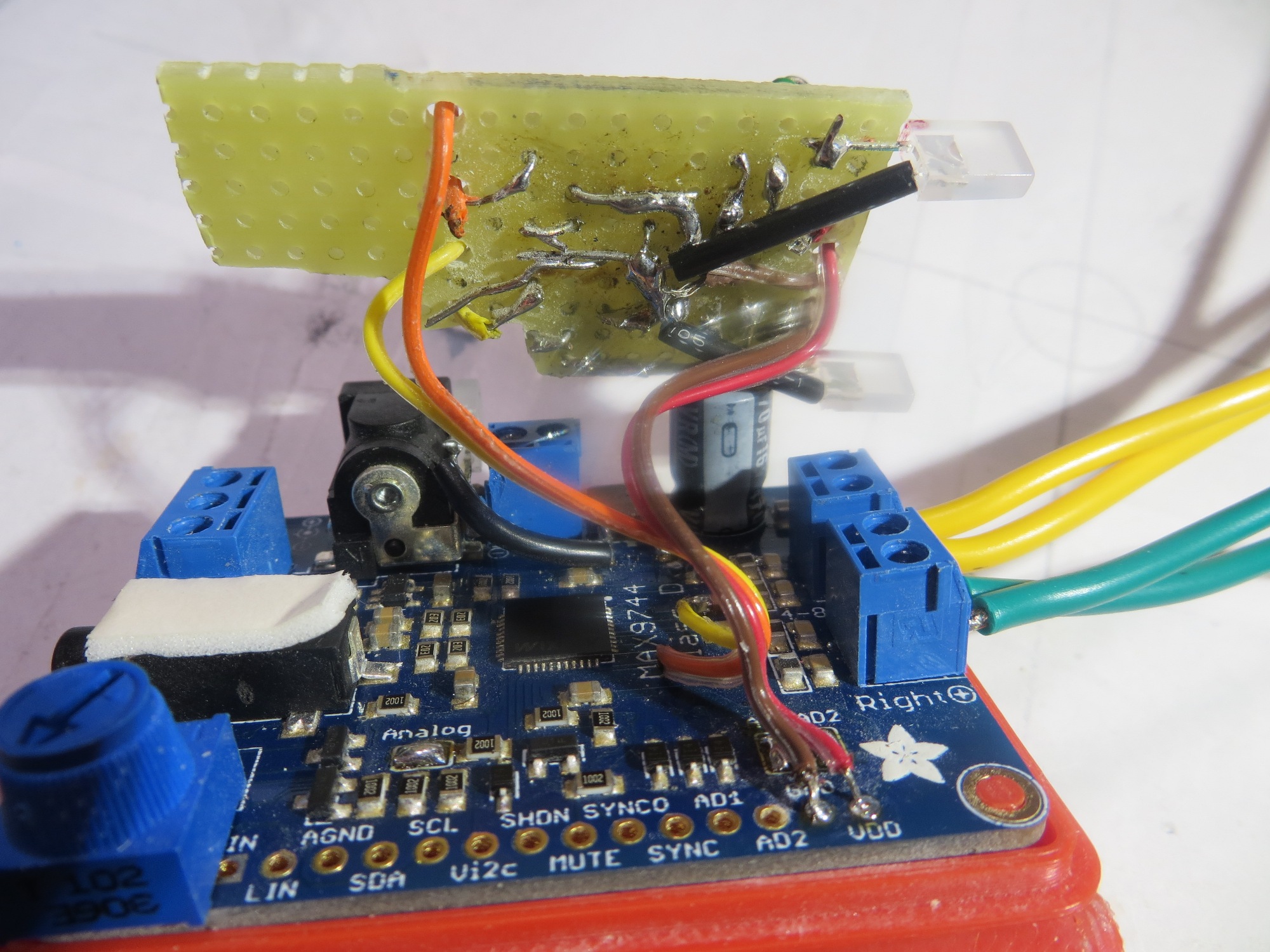
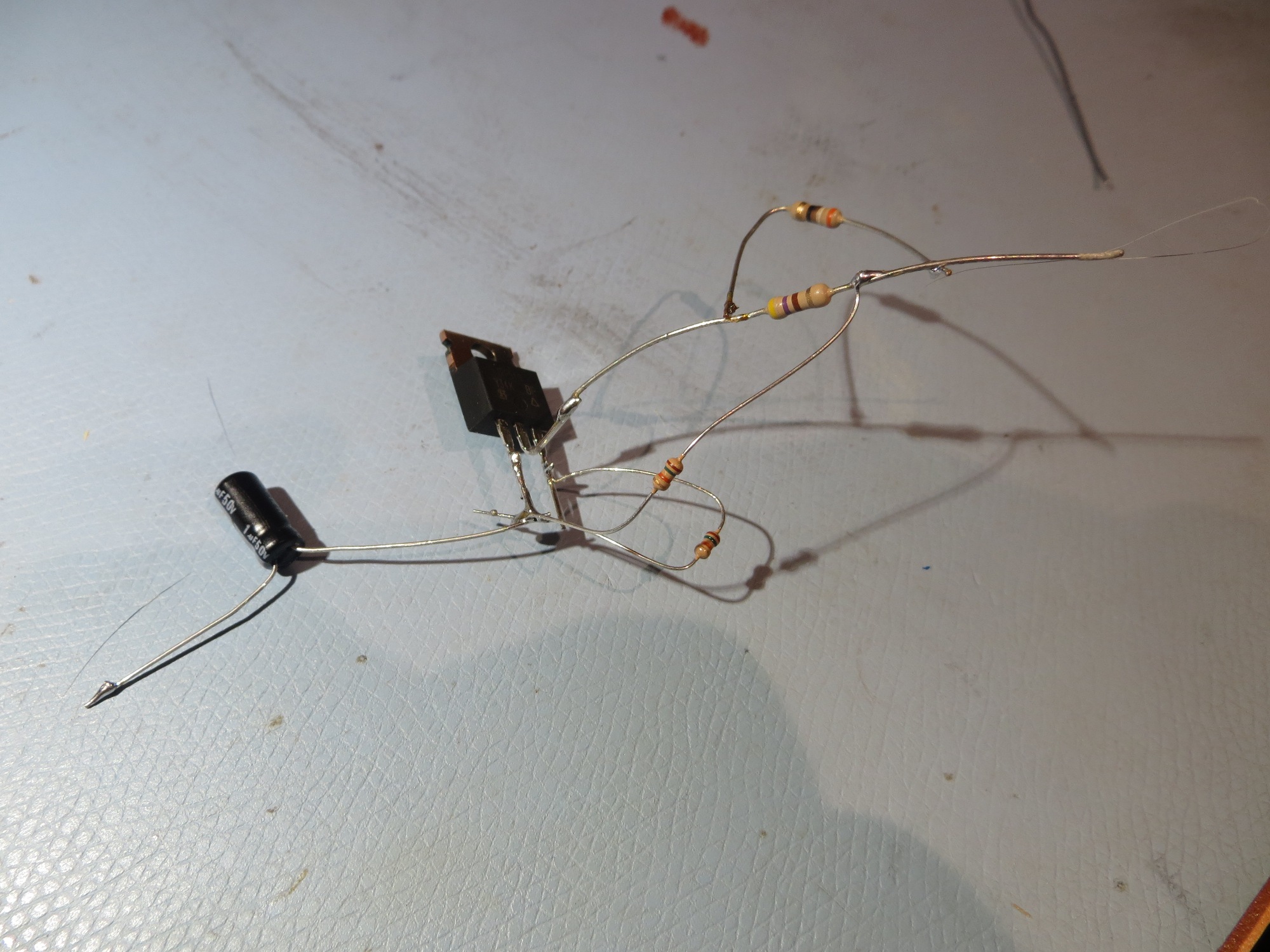
Sparkfun Pro Micro and HX711 board mounted on load cell

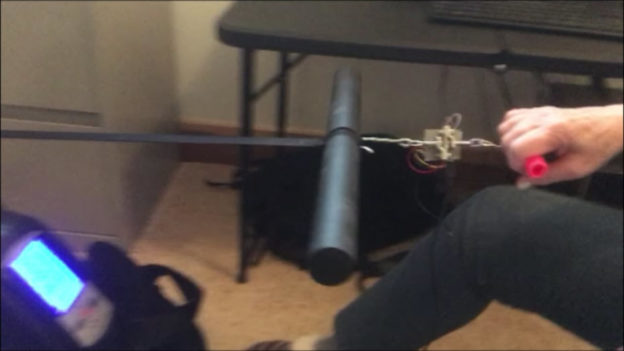
After getting all this set up, it was time to take some real data. Since I was still in the ‘no rowing’ zone after my surgery, I enlisted my lovely wife to do the honors while I recorded the data.   We have an Avari magnetic rowing machine, which thankfully doesn’t make much noise.   I recorded a total of 12 rowing cycles on two different ‘wave’ settings (I’m still not sure what the different ‘wave’ settings mean) at the lowest tension level, with the results shown below

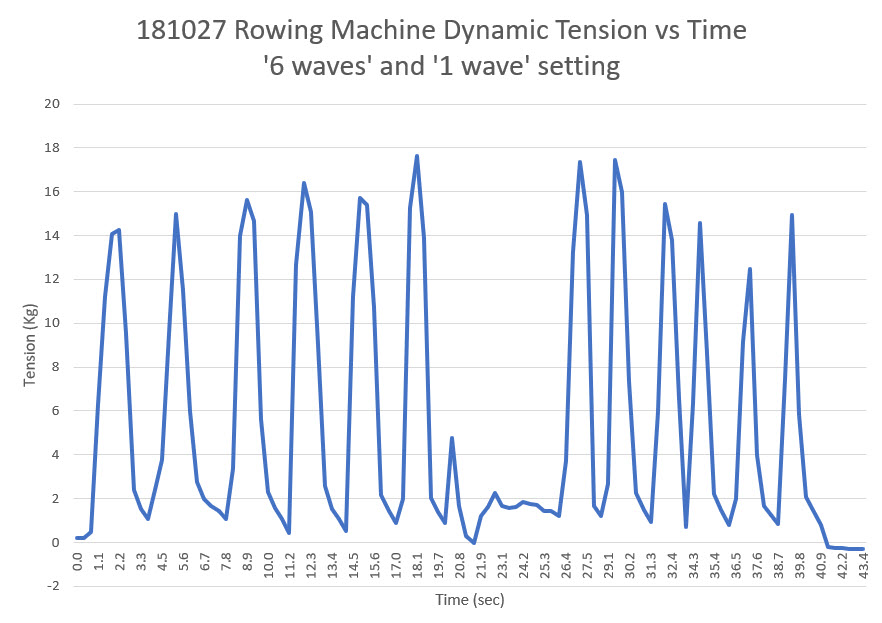
As shown in the above plot, the peak tension reading was around 18Kg (about 40 lbs).    I’ve included a short video of the test below.

IR Modulation Processing Algorithm Development. Part IV

Posted 07 June 2017

I seem to have grabbed a tiger by the tail in my continued collaboration with my old friend and mentor John Jenkins on this project to extract the estimated magnitude of a square-wave modulated IR signal in the presence of ‘flooding’ from ambient light sources.  The whole thing started out innocently enough when John was at our house a few weeks ago and I showed him my spiffy wall-following autonomous robot Wall-E2.  I mentioned at the time that I was having some trouble getting Wall-E2 to successfully home in on an IR beam to mate with a charging station, and he suggested that a square-wave modulated signal might do the trick, as it would allow me (and Wall-E2) to discriminate between the IR beam and the other interfering signals.

I should have known right then that I was in trouble, as John had that look in his eyes – the one that says “Hmm, that’s an interesting problem…..”.  I have seen that look any number of times over the 40 years or so that I have known him, and it  always results in me tearing up my previous work (and my previous assumptions) and starting over again.  The only saving graces in all this are a) It’s a  lot of fun when it happens, b) I’m retired now so I don’t care how long it takes or how much work is involved, and c) I’m a masochist at heart! ;-).

So, here we are.  John and I have been exchanging emails over the last week or so, discussing the ‘best’ way to solve this problem.  One of the first things that happened was John started blabbering about ‘Degenerate N-path Bandpass Filters’, and I had no idea what he was talking about (I  hate it when that happens!).  Of course I couldn’t tell John that I was completely ignorant, so I made the appropriate noises and raced to educate myself before he discovered my ignorance.  I found a neat video that explained the technique in a way that even I could understand. The video focused on implementing the filter technique in CMOS hardware, but the general technique is applicable to the Arduino world as well, as long as the modulation frequency is low enough to accommodate the lower clock speeds.

John came up with a brilliant graphical illustration of the algorithm used for implementing a N-path band-pass filter.  Even more amazing, he did it in Excel, so the whole damned thing is live – wow!   As shown in the ‘dead’ version below, there are two ‘channels’ – an in-phase (I) and quadrature (Q) ‘channel’.  Both channels start with a group of samples spanning exactly 1/4 cycle  that are summed together to form a ‘sample group’.  In the I channel, each group is given a sign in the sequence ‘+’, ‘+’, ‘-‘, ‘-‘, and in the Q channel this same group is given a sign in the sequence  ‘-‘, ‘+’, ‘+’, ‘-‘.  The four groups in each channel are summed to form the I & Q ‘cycle sums’, and each such sum is added to a N-element circular buffer (one each for the I & Q channels).  The running sum of all elements in each circular buffer are the band-pass filtered I & Q components of the input signal.  The final result is formed by adding the absolute values of the I & Q running sums.

Loader Loading...
EAD Logo Taking too long?

Reload Reload document
| Open Open in new tab

Download

Page 1 of the above document shows the sign sequence for the in-phase and quadrature ‘channels’.  Note that the input to both channels is the same ‘sum-of-5-samples’ group, but the sign changes in a different sequence for the I & Q ‘channels’.  Each 1/4 cycle of the input signal is treated in the same fashion.  The horizontal time scale is specific for the planned 500Hz modulation signal.

Page 2 depicts the real heart of the algorithm, as it shows how each ‘sample sum’ (1/4-cycle sum-of-samples) feeds into the final circular summing buffer.  Four ‘sample sum’ groups (comprising one signal cycle) are summed into a ‘cycle sum’ for both the I & Q channels, and each such ‘cycle sum’ is loaded into the corresponding I or Q circular summing buffer.  The latest ‘cycle sum’ element replaces the oldest element, and therefore the  circular summing buffer for each channel represents a N-element  band-pass filter, where N is the length of the circular summing  buffer.  This diagram has a  lot of information in it, so it can take some time to get comfortable with it (it did for me, anyway).

Some other random details:

  • This diagram is set up for a 64-element circular summing buffer, but shorter or longer is OK too.  The band-pass filter bandwidth is inversely proportional to the buffer length.
  • The times noted in the labels at the top are for a presumed 500Hz modulation, with a period of 2000uSec.
  • The notation m = n/5 comes from the fact that (in this particular implementation) there are 20 samples/cycle, which means that each 1/4 cycle group of contains 5 samples.  For 64 elements, each comprising 1 entire cycle of samples, there are 64X20 = 1280 samples. So in this implementation, m/4 = 64 ==> m = 256 = n/5 ==> n = 1280 total samples represented in the circular buffer at any one time.

Page 3 shows the contents of one of the two circular buffers, after each complete ‘rotation’ of the buffer.  After 64 complete cycles the buffer is full, as shown in the ’00’ column.  64 cycles later, the buffer contents are as shown in the ’01’ column, and so on.  The text below shows the procedure for start and running the buffer.  Note in this text that “next cycle value” and “current cycle value” are the same thing, and the “input pointer” and “output pointer” variables are incremented  MOD N, (N = 64 here).

Pages 4-12 show the input signal, the I/Q channel values, and the I & Q circular buffer running sums for different phase offsets between the transmitted and received signals (transmit & receive frequencies are the same in all cases).  Page 4, for instance, shows the situation for the receiver perfectly in phase with the transmitted signal.  If we look at the I & Q summed values at integral cycle boundaries (-1, 0, +1, etc) we see that the I signal is at 128, and the Q signal is at 0, giving abs(I) + abs(Q) = 128 + 0 = 128.  If the same calculation is performed for all the other phase relationships (i.e. pages 5-12) at the same points, the answer will always be the same, i.e. 128.  This shows that the band-pass filter implementation works as intended, even without any phase-locking requirement.  This treatment assumes that the Tx & Rx clocks are identical, so that the 1/4-cycle sample groups span exactly 1/4 cycle.  Any difference between the two clocks will show up as ripple on the results, proportional to the difference between the two frequencies.  This error term should not be significant for the typical single-board-computer crystal-controlled clocks.

I sent this post off to John for approval, and got the following email back, with some additional clarifying comments:

  • n-path filter is degenerate (my term) because it only uses two paths — I and Q — vice many as shown in video (very good video btw,learn a lot from it too)
  • possible topics for more detail  related to last paragraph (but beware that perfect is enemy of good enough or something like that):
    • output ripple
      • frequency ==> difference between tx and rx freqs should be very small
        • only spec found was +/-50ppm, so 100ppm delta worst-case w/o aging, etc
        • 100ppm at 500Hz ==> 0.05Hz
        • believe ripple will be twice difference in freq because of this being a fullwave synchronous rectifier (not verified), so 0.1Hz
      • magnitude  ==> variations due to sample(s) from one 1/4-cycle group getting into an adjacent 1/4-cycle group as tx and rx phases slide past each other at <<0.1cycle/sec
        • non-50/50 duty cycle is most likely cause
        • with 5-samples per 1/4-cycle group normalized ripple could vary from 1.0 to 0.8;
          • not a problem for the relative  outputs of two sensors for steering
          • could be important in cases where absolute magnitude is needed because bpf  (eg, 10Hz) would not average signal for long enough to average out ripple this slow ((eg, 1 cycle every 10sec)
          • increasing # of samples per 1/4-cycle group will reduce this effect
    • no antialias filter is used so # of samples  per 1/4-cycle group needs to be significantly higher than nyquist requirement for 2/bw to avoid issues (unless clock rate is servo’d to correct freq by monitoring and setting Q value to zero)

More to come – stay tuned!

Frank


How to update the ACP Pyramid

The first thing to understand about updating the Pyramid is that you don’t have to unless there is something wrong with your current Pyramid version (i.e. there is a
a bug or problem) that has been addressed in the latest version available on the ACP website).  As each new version is placed on the ACP website, a ‘change log’ entry is also uploaded, so you can tell what changed from your current version to the one that is on the website. If none of the listed changes affect your practice, then there is no real need to update.

the second thing to understand about updates is that, even if you download the latest version from the ACP site, there is no need to immediately update all your client Pyramid files – it is completely reasonable to update client Pyramids to the latest version only when you next deal with a particular client file, and this is done by simply importing the client’s Pyramid data into the new (blank) version using the ‘Import from File…’ button on the Inventory page (don’t forget to use ‘Save As…’ to save the updated client file back to the client folder while leaving the new version file unchanged).  Here’s a video tutorial showing the update procedure

OSU/STEM Outreach Pulse Detector Project, Part II

Posted 22 October, 2016

In my last post on this subject, I discussed a modification to the OSU STEM Outreach’s Pulse Detector schematic to eliminate the dual 9V battery supply in favor of a single one, taking advantage of the LM358 op-amp’s single supply operation capability.  However, before actually recommending that the new arrangement be adopted, I wanted to make sure that it would work properly with the OXO ‘Soft-Clip’ finger clip module instead of the one I created for testing in my lab.  It  should work, but as a long-time engineer I have been bitten more than once by the difference between  should and  would! ;-).

So, Prof Anderson was gracious enough to bring a spare OXO clip to our next Outreach session, and since then I have had the opportunity to test this clip with my new circuit, as shown in the following photo.

OXO 'Soft-Clip' finger clip with new circuit in background

OXO ‘Soft-Clip’ finger clip with new circuit in background

After fiddling with the tension screw a bit, I got the Soft-Clip tension set properly for my finger, and lo-and-behold, the pulse detector circuit worked out quite nicely, as shown in the following short video clip (as you watch the clip, note that the IR beam from the IR LED is visible as a blue-white glow).

At this time I also made one other minor change.  In the original OSU circuit, the DC blocking capacitor (C2 in the schematic) was a 0.1uF, but in my circuit this value was changed to 0.01uF, because that’s all I had on hand.  In the meantime, however, I got some 0.1uF’s from Mouser, and so my final circuit as shown above incorporates a 0.1uF vice the original 0.01.

The next step in this project is to transfer the detector circuit from plugboard to a more permanent version on perfboard.  This will allow me to demonstrate the new circuit to Prof Anderson and the rest of the OSU STEM Outreach team, to lend credence to the idea of modifying this project’s documentation to eliminate the now-unneeded second supply.  Stay tuned!

Posted 10/24/2016

So, tonight I had the time to finish transferring the pulse detector circuit from my old trusty plugboard to a more permanent medium – i.e. perfboard.  The idea here is to provide the OSU STEM Outreach team with a working pulse detector circuit running from a single 9V battery, as a working example of my recommended modifications to the  circuit being used presently.  The image below shows the perfboard arrangement, and there is also a short video clip of the new pulse detector circuit in action.

The astute observer might notice there are only three wires going from the OXO ‘Soft-Clip’ assembly to the pulse detector circuit.  While I was wiring up the perfboard version, I realized I could eliminate one wire by simply moving the 100-Ohm IR LED current-limiting resistor from the anode (positive) side of the diode to the cathode (negative) end. This allowed me to connect the IR LED anode to the PhotoDiode cathode, and both to the +9V lead.  Implementing this change for all of the current stock of OXO clips may be more than the OSU STEM Outreach crew wants to take on, but I thought I would mention it ;-).  The finished schematic (with the transposed 100-Ohm resistor) is shown below

Final pulse detector schematic.  Note change to IR LED current limit resistor, and DC blocking capacitor

Final pulse detector schematic. Note change to IR LED current limit resistor, and DC blocking capacitor


Perfboard version of the single-supply pulse detector circuit

Perfboard version of the single-supply pulse detector circuit

The next (and hopefully final) step in all this is to 3D print a small box for the perfboard circuit.  Because I can’t help myself, I have decided to try printing  a transparent box – not a trivial undertaking for 3D printing.  Stay tuned!

Posted 10/25/2016

As mentioned above, 3D printing a transparent box is a non-trivial undertaking, at least with the current hobbyist FDM (Fused Deposition Modeling) materials and techniques.  After a number of iterations, the best I could do without a  lot of post-processing was a semi-transparent (but still pretty neat) container for the perfboard version of the ‘new-and-improved’ OSU Pulse Detector circuit.

As I have noted previously, the current 3D printing technology makes it easier, faster, and cheaper to go through a number of test cases (literally in this ‘case’!) on the way to a final product, rather than trying to design a final product all in one crack.  Each test takes about 15-30 minutes and just a few cents’ worth of material, and quite often the iterative process illuminates a design problem or opportunity that wasn’t obvious (or even considered) at the start.  In this case, it became apparent after about the 4th iteration that the perfboard should be mounted to the ‘lid’ via printed-on standoffs rather than to the ‘bottom’.

The TinkerCad model for the box and the lid is shown below, as well as the finished product and some of the precursor test boxes.  And, as usual, a short video of the final product.

Pulse Detector Box and lid. Note printed-on standoffs

Pulse Detector Box and lid. Note printed-on standoffs

OSU Pulse Detector Box and precursors

OSU Pulse Detector Box and precursors

Frank


OSU/STEM Outreach Pulse Detector Project


Posted 10/16/2016

A week or so ago I participated in an OSU STEM Outreach program that showed high-school students how to build a working pulse detector circuit, using a commonly available op-amp and an IR LED/Photodetector pair.  After an initial presentation, the students were given step-by-step instructions for building the circuit on a small plugboard, and I helped when students ran into trouble.  By the end of the one-hour session, most students were successful, and were able to see the output LED illuminate in time with their pulse – cool!

As I helped out with the class, I was a bit shocked to see that the circuit being build by the students required two 9V batteries wired in series to create a +/-9V supply for the op-amp. At the time I just assumed somebody forgot to spec the op-amp to be one with a common-mode range including ground, and the extra battery was the ‘field-expedient fix’ for the problem. When I asked Prof. Betty Lise Anderson about this, she said that a single supply had been tried at one point, but ‘didn’t work out’ for unspecified reasons.   This piqued my interest, so  decided I would investigate the problem a bit further in my home lab.

As it turned out, the op-amp being used in the students’ circuits was the ubiquitous dual-LM358  in an 8-pin DIP, and this unit does indeed have a common-mode range including ground, so  the single-supply idea should have worked.  Here’s the original OSU circuit (transcribed into DipTrace’s schematic capture format)

Original OSU Pulse Detector circuit.  Note the dual 9V suppies

Original OSU Pulse Detector circuit. Note the dual 9V suppies

And here’s my final single-supply detector circuit

Final single-supply Pulse Detector schematic

Final single-supply Pulse Detector schematic

Comparing the two, the only real difference is the addition of the 470K resistor from the inverting input to ground.  In the original circuit, the inverting input was tied directly to ground, while the non-inverting input had a 470K to ground.  This can be a problem, as the input bias current for the LM358 can be on the order of 100 X 10-9 (100 pico-Amp), which means that the DC voltage at  the non-inverting input due to bias currents could be as much as 50mV or so.  Since this is on the same order of magnitude as the photo-diode signal at this point, there is a real chance the op-amp would never toggle the output.  The dual-supply setup  eliminates  this problem, but at the cost of a second battery.

The final circuit, as laid out on my plug-board, is shown below.

Pulse Detector circuit with my 3D-printed finger socket

Pulse Detector circuit with my 3D-printed finger socket

Final Pulse Detector circuit

Final Pulse Detector circuit

And, because I can, here’s a short movie showing the pulse detector in action ;-).

Speaker Amplifier Project, Part V

Posted 10 September 2016

Since my last post on this subject, I have actually gone through two revs of the PCB. The first set was fine electrically (and great quality AFAICT, but I didn’t get the physical border just right, and  I couldn’t file it down enough to fit without breaking a PCB run.  So, I went back to DipTrace, redid the board outline (which also involved some rejiggering of component placement and a bit of manual net editing) and sent off another order to Bay Area Circuits.  After returning from  a week at a duplicate bridge tournament in Atlanta  with my wife, the new rev boards were waiting for me – cool!  The image below shows the new board as installed on the Adafruit 20W amplifier board.

Rev2 PCB installed on Adafruit amplifier

Rev2 PCB installed on Adafruit amplifier

After ensuring that the PCB fit was OK, I populated it, checked all the net connections and resistor values and gave it the old smoke test – and of course it failed – ugh!  I quickly found that the problem was that common-mode range of the the MC748 dual op-amp I was using for the second system doesn’t include ground – oops!  A quick trip to the local Microcenter and the purchase of a wildly overpriced NTE928 dual op-amp solved that problem, but because I was I had soldered the op-amp package directly onto the board (I was  sure this was all going to work, after all), I was now faced with a messy removal and cleanup job.  After getting the old op-amp off and the PCB cleaned up, I installed the new one  (this time, suitably chastised, I installed a socket, and  then installed the op-amp).  The following image shows the finished PCB connected to the amp board, next to the hand-wired original.

Completed PCB connected to Adafruit amplifier

Completed PCB connected to Adafruit amplifier

Bottom of PCB and hand-wired original (note messy area around op-amp)

Bottom of PCB and hand-wired original (note messy area around op-amp)

The last thing to do was to get the PCB actually mounted onto the amplifier board, and the assembly into its custom-printed housing, as shown in the following images.

hand-wired and Rev2 PCB mounted to the Adafruit amp boards

hand-wired and Rev2 PCB mounted to the Adafruit amp boards

hand-wired and rev2 PCB mounted in custom-printed enclosures.

hand-wired and rev2 PCB mounted in custom-printed enclosures.

Now all I need is a ‘speaker’ presentation so I can find out if all this work was really worthwhile (actually, I’ve already had a great time with this project, so having it actually work for the students will just be icing on the cake!)


OSU/STEM Outreach Speaker Amplifier Project, Part IV

Posted 04 August, 2016

In my last post on this subject, I described the finishing touches on the project to design and fabricate a speaker amplifier for the OSU Engineering Outreach ‘paper speaker’ student project. The ‘finished’ project featured an audio activity monitoring circuit piggybacked onto the Adafruit 20W Class-D amplifier board, using my almost-forgotten  hand-wiring techniques on fiberglass ‘perf-board’, as shown in the following images.

Cut-down perfboard, top view

Cut-down perfboard, top view

Cut-down perfboard, bottom view

Cut-down perfboard, bottom view

While this technique is perfect for a one-off project, I ultimately wanted to fabricate a number of these amplifier/monitor modules for use by the OSU Engineering Outreach team.  So, I decided to investigate the feasibility of obtaining a printed-circuit (PCB) board version of the LED monitor circuit, so I wouldn’t have to hand-fabricate the same circuit multiple times.  Of course, I knew in my heart that I could probably hand-fabricate ten (or a hundred) LED monitor circuits in the time it would take me to research the PCB design/fabrication field, acquire and learn a PCB design (aka EDA) package, actually design and implement the PCB, and then have the boards fabricated by a PCB house, but where’s the fun in that?

The last time I dealt with PCB design and manufacture was about 15 years ago while I was a researcher/JOAT (look it up) at The Ohio State University ElectroScience Laboratory, a research lab that specializes in Electromagnetics research and applications.  At the time I was a relatively new grad student at the lab (but one with about 30 years of electronics design  experience  in a prior lifetime with the CIA) and had somehow managed to get involved in a project that required some small-quantity PCBs.  The lab’s normal supplier (a local PCB manufacturing house) was still using hand-taping methods and the result was very high priced and of somewhat inconsistent quality (at least in my opinion), so I started looking for ‘a better way’.  In short order I found some low-cost, high quality EDA tools, and also found a small PCB house in Canada that would deliver small quantities in about 1/10 the time and 1/10 the cost as the local house. This made me a hero in the eyes of the lab director (but an enemy in the eyes of the guys who were comfortable dealing with the local supplier).  Anyway, it’s been another decade or so since I last looked at the EDA/PCB field,  so  I suspected things were even better now – and I wasn’t disappointed!

After a few hours of Googling, I found a number of posts that indicated that one of the better/easier-to-use EDA packages was Dip Trace, and they had a freeware version for those of us who can get by with 300 pins or less and only 2 signal layers – YAY!!  With a little further digging, I found some very complimentary reviews, so I downloaded the ‘free’ version and started trying to refresh  my PCB ‘game’.  Right away I found that DipTrace has a very complete and readable beginner’s tutorial, and unlike most ‘tutorials’ these days, the DipTrace one doesn’t skip steps – everything is explained and demonstrated in what had to seem like completely unnecessary detail to the experts, but in fact is absolutely crucial for a (almost) first-timer like me. If you are a hobbyist/enthusiast interested in PCB design/fabrication, I highly recommend DipTrace.

After working my way through most of the tutorial, I decided to try my hand at implementing my LED monitor circuit.  I started by porting my schematic from Digikey’s ‘scheme-it‘ (a free, browser-based schematic capture utility).  Here’s the schematic – first from Scheme-It, and then as it was ported to DipTrace.

LED Monitor circuit schematic as captured in Digikey's 'Scheme-It' app

LED Monitor circuit schematic as captured in Digikey’s ‘Scheme-It’ app

LED Monitor circuit schematic as captured in DipTrace

LED Monitor circuit schematic as captured in DipTrace

Following the procedure described (in exhaustive detail – YAY!) in the DipTrace tutorial, I then created an initial PCB design using ‘File -> Convert to PCB’ (or Ctrl-B) in the schematic capture app. This launches the PCB designer, and presents an initially disorganized parts layout as shown below.

Initial PCB layout

Initial PCB layout

Had it not been for the great tutorial, this mishmash of parts would have been a real turnoff; fortunately, the tutorial had already covered this, so I knew to ‘keep calm and carry on’ by selecting ‘Placement -> Arrange Components’ from the main menu, which resulted in this much more compact and reasonable arrangement.

After 'Placement->Arrange Components'

After ‘Placement->Arrange Components’

Working back and forth between the tutorial, the actual Adafruit 20W amplifier board, and the PCB design/layout screen, I was able to arrive at a final PCB design that implemented the entire circuit in a form factor that fit into the space available, as shown below.

Finished PCB layout. Note the purple board border is customized to fit on top of the Adafruit amp board

Finished PCB layout. Note the purple board border is customized to fit on top of the Adafruit amp board

The above layout was significantly customized to fit on top of the Adafruit 20W amp board and in the 3D-printed enclosure.   This required a number of iterations, but the process was well supported by DipTrace; in particular, the ability to print the layout on my local laser printer in 1:1 scale helped immensely, as I was able to cut it out with scissors and actually lay it on top of the amp board to check the fit.

I was curious about how close I came to the ‘free’ version limitation of 300 pins, so I displayed the ‘File->Layout Properties’ dialog as shown below.  From this it was obvious that I still have plenty of room to play with for future projects, although I did use both the available signal layers. ;-).

PCB properties, showing that this design fits well within the 300-pin maximum for the 'free' version

PCB properties, showing that this design fits well within the 300-pin maximum for the ‘free’ version

All in all, I probably spent 2-3 days from start to finish with DipTrace to get a finished PCB layout – not too shabby for an old broke-down engineer who can’t remember where he left his cane and hearing aids ;-).

But, all of this wasn’t even the really cool part of working with DipTrace!  The  really cool part came when I realized that DipTrace features a ‘baked-in’ link with Bay Area Circuits  for PCB procurement (File -> Order PCB…) as shown below

The 'File->Order PCB' menu item

The ‘File->Order PCB’ menu item

When you click on this option, the relevant data is scarfed up from the PCB layout information and you are presented with a simple ordering screen, complete with per-unit and total prices for your design.  All you have to do is select the quantity desired and press the ‘Place Order…’ button.  No messing with Gerber files, net lists, drilling schedules, mask layouts, etc etc.  One button, 30 bucks from my PayPal account – done!!!

The order detail screen

The order detail screen

So, the lead time on the board order was quoted as about 10 days, so I won’t know for a couple of weeks how the whole thing worked out, but I’m quite optimistic.  I have to say that this was the most pleasurable and trouble-free PCB design project I have ever experienced, and I have experienced  a lot of them over the last 50 years, from hand-cut 10X mylar PCB masks, to hobbyist acid-baths, to $10,000 setup charge custom PCB shops, to this – wow!  I may never do another PCB project, but if I do, DipTrace will be my drug of choice!

Stay tuned,

Frank


OSU/STEM Outreach Speaker Amplifier Project, Part III


Posted 29 July 2016,

In my last post on this subject, I described the work to be completed to finish the OSU/STEM Outreach speaker amplifier project, as follows:

  • physically cut the perfboard down to a size that will fit into the enclosure, and figure out how it is to be secured.
  • Figure out how to mount the channel monitor LEDs so that they can be seen from outside the enclosure.  The plan at the moment is to mount them on the outside edge of the left and right screw terminals, respectively, and widen the AUD OUT opening enough so they can be easily viewed from outside.
  • Figure out how to route power and audio signals to the LED monitor board without using the external power and audio output screw terminals. The power wiring should be simple, as power and ground are available on the breakout pins provided by Adafruit.  However, the audio output signals are more problematic, as it isn’t obvious how to get to these circuit points, and I  really don’t want to start drilling holes in a multi-layer PCB.  After a careful visual inspection and some probing with my trusty DVM, I think I have located where I can safely tap into the PCB run from the last SMT resistor to the positive audio terminal for each channel – we’ll see!
  • Make sure the enclosure top fits OK, and all three LEDs are indeed visible.
  • Install semi-permanent L/R audio output cables with alligator clip terminations.  In actual use, I don’t really expect two paper speakers to be connected at once, but I’ll be ready if that situation occurs ;-).

Cut the perfboard down (and mount the LEDs):

With the help of my trusty Dremel tool and a carbide cutoff wheel, I trimmed the perfboard down to a size and shape that would fit into the enclosure, using the top surface of the audio input jack as a handy mating surface on one end, and with the monitor LEDs themselves as mounting legs on the other end, as shown in the following photos.

Cut-down perfboard, mounted front view

Cut-down perfboard, mounted front view

Cut-down perfboard, mounted, side view

Cut-down perfboard, mounted, side view

Power and audio signal wiring:

160729_LEDMonitorBoard1

Audio and power wiring

Audio and power wiring

Enclosure:

160729_LEDMonitorEncl4

Completed project shown connected to OSU paper speaker

Completed project shown connected to OSU paper speaker

Speaker connection cables:

Enclosure side view showing audio output connections

Enclosure side view showing audio output connections

All  Together Now…


So, at this point the amplifier project is all done  except for the ‘proof of the pudding’, which in this case is a real field test with real participants and student helpers.  If the field test results are satisfactory, I’ll probably build at least two more complete systems (I got 3ea amp boards from Adafruit and haven’t managed to kill any of them yet), and donate them to the OSU Engineering Outreach project.

Frank


OSU/STEM Outreach Speaker Amplifier Project, Part II

Posted 27 July 2016

In my last post on this subject, I had gotten to the point where I had a single-channel LED monitor circuit working, although it was still a bit  unkempt, to say the least.  In this post I describe the effort to get both channels working and to neaten everything up prior to installing the circuit into the speaker amplifier enclosure.

First off, I ‘improved’ the LED monitor circuit a bit, based on the results from testing the one-channel version.  I discovered there was a DC term riding on the class-D input signal, and this was getting amplified through the LED monitor circuit and swamping the audio  output at the LED.  So I added a 0.01uF DC blocking cap on the input line.  Unfortunately, this caused another problem, in that now the RC circuit cap had no discharge path so it almost immediately charged up and again swamped the audio signal.  One more addition – a 330K Ohm resistor across the low-pass cap to allow it to discharge.  Then, I adjusted the DC gain of the amp to provide a good  LED response to the audio.  I wanted the LED’s to come alive just about the time that a well-fabricated speaker produced clearly audible output.  The idea here is that a helper can tell immediately from the LEDs whether or not there is sufficient output power present to produce an audible response, and therefore if no response is detected, there is a problem with the speaker or the wiring from the amp to the speaker – but not upstream of that point.  After some fiddling around, I settled on a gain of about 70 for the LED monitor.  With that setup, and with the 20W amp gain set appropriately, I could easily drive the OSU paper speaker from my laptop, with the laptop’s audio output slider at about 50%.  The ‘New Improved’ LED monitor circuit is shown below:

Revised LED monitor schematic - one of two channels shown.

Revised LED monitor schematic – one of two channels shown.

The audio input to the monitor circuit is the rail-to-rail high-frequency (about 300KHz) audio-modulated PWM signal, as shown below

Amplifier output with audio input signal present

Amplifier output with audio input signal present

After the RC filter, only the audio signal is present, as shown in the following photo

LED monitor circuit audio input. Scope is set to 200mv/div

LED monitor circuit audio input. Scope is set to 200mv/div.

The following photo shows the output.  Due to the use of a single-supply op-amp and without any DC bias arrangement, only the positive input signal excursions produce an output – but that’s OK in this circuit as all we are doing is driving an LED.

LED monitor circuit LED drive signal. Only the positive audio transitions produce an output. Scope set to 2V/div

LED monitor circuit LED drive signal. Only the positive audio transitions produce an output. Scope set to 2V/div

While tweaking the monitor circuit, I had made quite a mess of my little perf-board layout.  So, after getting the schematic in good shape I basically tore everything down and started over again with the aim of building up the two-channel layout.  After everything was done, the result was the circuit shown in the following photo

Two-channel LED monitor circuit detail

Two-channel LED monitor circuit detail

two-channel LED monitor circuit in operation with the Adafruit 20W amp and the OSU paper speaker

two-channel LED monitor circuit in operation with the Adafruit 20W amp and the OSU paper speaker

After re-working the perf-board layout, adding the second channel, and carefully checking the wiring against the circuit, I was pleased to see that both channels operated as desired, and either channel could easily drive the OSU paper speaker.  The following short video shows the speaker being driven by the right channel, and both channel signals being monitored by the LED monitor circuit.


At this point the remaining work is:

  • physically cut the perfboard down to a size that will fit into the enclosure, and figure out how it is to be secured.
  • Figure out how to mount the channel monitor LEDs so that they can be seen from outside the enclosure.  The plan at the moment is to mount them on the outside edge of the left and right screw terminals, respectively, and widen the AUD OUT opening enough so they can be easily viewed from outside.
  • Figure out how to route power and audio signals to the LED monitor board without using the external power and audio output screw terminals. The power wiring should be simple, as power and ground are available on the breakout pins provided by Adafruit.  However, the audio output signals are more problematic, as it isn’t obvious how to get to these circuit points, and I  really don’t want to start drilling holes in a multi-layer PCB.  After a careful visual inspection and some probing with my trusty DVM, I think I have located where I can safely tap into the PCB run from the last SMT resistor to the positive audio terminal for each channel – we’ll see!
  • Make sure the enclosure top fits OK, and all three LEDs are indeed visible.
  • Install semi-permanent L/R audio output cables with alligator clip terminations.  In actual use, I don’t really expect two paper speakers to be connected at once, but I’ll be ready if that situation occurs ;-).

Once I’m sure everything is working OK and that the whole thing won’t die on me the first time someone looks at it sideways, then the plan is to volunteer for an upcoming speaker fabrication session and try the amp in the ‘real world’.  If it works as I fully expect it to, then the idea is to donate two or three to the OSU Engineering Outreach program, in the name of my company (EM Workbench LLC).  Stay tuned!

Frank


OSU/STEM Outreach Speaker Amplifier Project, Part I

Posted  July 25, 2016

Lately I have become involved in the Engineering Outreach program here at The Ohio State University, as a volunteer helper at ‘hands-on’ engineering project presentations to grade-school and middle-school students in the Columbus, Ohio area.  A week or so ago I helped out in a session where the students (middle-schoolers at a science day-camp) got to fabricate and test an audio speaker from a paper template, some magnet wire, and a couple of small permanent magnets, and I was struck by the difficulty the kids were having in actually hearing anything coming out of their freshly-fabricated speakers when they connected them to the output of their phones and/or iPads.  I could understand if I couldn’t hear anything – I’m an old power pilot and my ears are shot from thousands of hours of piston engine noise – but the kids with their brand-new ears couldn’t hear anything either!  There was an audio amplifier available for the kids to use, but it wasn’t much help either – there wasn’t any indication that the amp was actually doing anything, so it could have died long ago and nobody would ever know – bummer.  Anyway, I came away from that project with the distinct impression that this particular project wasn’t doing much for the kids, and maybe I could do something to help.  So, before I left the room, I made a point of ‘borrowing’ all the parts required to fabricate my own paper speaker – the paper template, magnet wire, and permanent magnets along with the other small bits and pieces.

My first line of inquiry in my own home lab was to determine what the best fabrication technique was for the speaker itself.  My thinking was that since this project has been around forever in one guise or another, it sorta  had to be successful in some sense, or it would have died out long ago.  Therefore, I reasoned that a more careful approach to the actual fabrication might yield better results.  After doing some inet research, I realized that one of the critical aspects of paper speaker construction is to make sure the speaker coil assembly (a section of plastic straw hot-glued to the speaker cone with the magnet wire wound around it’s lower end) was free to move vertically – i.e. it wasn’t forced down against the baseplate by the tension of the speaker legs.  In other words, the speaker legs had to be arranged such that the speaker coil assembly floated 2-3  mm above the base.  After playing with this a while, I realized that the proper technique was to arrange the speaker legs so as to properly suspend the coil assembly first, and then place the permanent magnet ‘dot’ under the coil assembly second, rather than the other way around.  Assembly in this sequence tends to minimize lateral friction of the coil assembly straw section against the side of the permanent magnets, hopefully resulting in higher mechanical/audio transfer efficiency.

After constructing the speaker as carefully as possible, I hooked it up to my laptop audio output, and voila! – no audio :-(.  Even with the audio output at max volume (which, when directed to my laptop’s internal speakers is enough to vibrate my workbench), it was almost impossible to hear anything from the speaker.  Even with careful construction with no time constraints, and a top-end audio source, getting the speaker to work was a very marginal deal.

After thinking about this for a while, I decided that I was maybe working the wrong end of the system.  What I needed to do was to implement an audio amplifier that would provide sufficient output power so that even a marginally constructed speaker would work properly; the only real limitation on power that I could see would be the current limit imposed by the magnet wire itself – as long as I didn’t physically melt the wire, I should be OK! ;-).

My first try at an amplifier was based around a power MOSFET I had lying around, as shown in the following photo.  1607_MOSFET_AMP

This worked ,but only up until the point at which the drain resistor started smoking!  That’s the problem with a linear amplifier driving a speaker – LOTS of power being dissipated.

So, back to the drawing board, with more inet research.  This time, I came across the  very nice Adafruit  Class-D speaker amplifier  shown below.  The kit has everything needed to build a complete speaker amp, as shown in the second image below.  The amplifier runs Class-D, so it is very efficient, and it depends on the speaker coil inductance to  reject the high-frequency switching signal, leaving only the audio.


Adafruit 20W Class-D speaker amplifier, based on the MAX9744 amplifier chip

Adafruit 20W Class-D speaker amplifier, based on the MAX9744 amplifier chip

Adafruit 20W Class-D speaker amplifier application

Adafruit 20W Class-D speaker amplifier application

The folks at Adafruit were even thoughtful enough to provide the STL file for a 3D-printable enclosure for the amp, as shown below:

3D-printable enclosure for the 20W Class-D amp

3D-printable enclosure for the 20W Class-D amp

And, since I am the proud owner of not just one, but  two 3D printers (a Printrbot Simple Metal, and a PowerSpec 3D Pro/aka Flashforge Creator X), the existence  of a ready-made design for the enclosure saved some time.

After receiving my amps from Adafruit, and after the requisite amount of fumbling around, I managed to get the amp running and connected to a couple of old speakers.  When I connected up my laptop’s audio output I was quite pleased that, even at the default 6dB gain setting, the amp easily drove the speakers to the point where I had to reduce the audio input volume to avoid complaints from the wife in the next room.

Adafruit amp test setup

Adafruit amp test setup

At this point, it was clear that the Adafruit amp should be an excellent solution to the paper-speaker driver problem, but I wasn’t quite done yet.  There were still several  remaining issues:

  • The amplifier used in the previous sessions had no ‘power ON’ indication, so there was no way to tell if the thing was actually operating or not.  The Adafruit amp, as delivered doesn’t have one either, so this had to be corrected somehow.
  • The previous amplifier had no ‘audio activity’ indication, so even if you somehow knew that it was indeed getting  power and working, there wasn’t any way to tell if there was any audio output without  attaching a speaker; and if there was no sound, there was no way to tell if the problem was the speaker or the amp.
  • The original enclosure design by Adafruit didn’t actually fit – the slots for the power and audio-in jacks weren’t high enough (later design change?). In addition, there were no provisions for either the ‘power ON’ or ‘audio activity’ indicators.  Fortunately I not only have 3D printers, but an account on TinkerCad  so the design could be adjusted.
  • Since I still haven’t actually connected the amp to my paper speaker, I don’t really know yet if the default 6dB gain setting is sufficient to drive the speaker; I may still have to change to the analog gain setup and use a higher gain setting (fortunately, Adafruit thoughtfully provided a 1K potentiometer and a set of jumper pads to achieve this, if necessary).

Power-ON Indication:

The power-ON indication issue was fairly easy to address – all I had to do was add an LED-resistor combination across the external power input lines.   The only problem with this solution was finding a way for the LED to be visible outside the enclosure – and the solution was to modify the enclosure design to expose the external power screw terminals (they were hidden in the original design), and in the process leave a bit of space open between the power input jack  and the screw terminal, a space just wide enough for a small, rectangular LED as shown below.

Power ON indicator LED installed between power input jack and external power screw terminals

Power ON indicator LED installed between power input jack and external power screw terminals

Audio Activity Indicator:

The Adafruit amplifier is Class-D – i.e.  the output is a pulse-width-modulated (PWM) signal, as shown below:

Amplifier output with audio input signal present

Amplifier output with audio input signal present

Amplifier output with no audio input signal present

Amplifier output with no audio input signal present

As can (or more accurately,  cannot) be seen from the above photos, there is no appreciable difference between the ‘audio’ and ‘no audio’ waveforms.  The class D amplifier technique depends on the low-pass nature of the speaker coil to suppress  the high-frequency switched waveform  terms, leaving only the audio term.  Unfortunately, this means there really isn’t anything there to directly drive an audio activity indicator – the typical LED is plenty fast enough to follow the high-frequency PWM waveform, thereby masking the audio signal.  One possible technique would be to sample the speaker coil current (which pretty much by definition doesn’t contain the high-frequency switching terms), but this requires that a working speaker be attached.  This won’t work, because the whole idea of an audio activity indicator is to confirm that an audio input is present and has been amplified sufficiently to adequately drive a speaker  before one is connected.  So, I decided to try a simple RC low-pass filter, followed by a basic audio amplifier to drive the activity LED.  The circuit for one channel is shown below.

LED monitor circuit for one channel

LED monitor circuit for one channel.  Pin numbers are Channel1/Channel2

Here is a short video showing the LED monitor circuit in action


So, at this point I have a working speaker amplifier, a power-ON indicator, and at least the prototype of an audio activity monitoring circuit.  Next up – finish the LED monitor circuit, finish the enclosure design and fabrication, and assemble everything for delivery.