
Posted 10 September 2016
Since my last post on this subject, I have actually gone through two revs of the PCB. The first set was fine electrically (and great quality AFAICT, but I didn’t get the physical border just right, and I couldn’t file it down enough to fit without breaking a PCB run. So, I went back to DipTrace, redid the board outline (which also involved some rejiggering of component placement and a bit of manual net editing) and sent off another order to Bay Area Circuits. After returning from a week at a duplicate bridge tournament in Atlanta with my wife, the new rev boards were waiting for me – cool! The image below shows the new board as installed on the Adafruit 20W amplifier board.
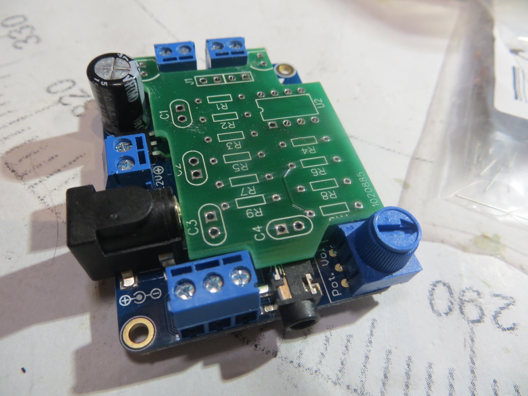
Rev2 PCB installed on Adafruit amplifier
After ensuring that the PCB fit was OK, I populated it, checked all the net connections and resistor values and gave it the old smoke test – and of course it failed – ugh! I quickly found that the problem was that common-mode range of the the MC748 dual op-amp I was using for the second system doesn’t include ground – oops! A quick trip to the local Microcenter and the purchase of a wildly overpriced NTE928 dual op-amp solved that problem, but because I was I had soldered the op-amp package directly onto the board (I was sure this was all going to work, after all), I was now faced with a messy removal and cleanup job. After getting the old op-amp off and the PCB cleaned up, I installed the new one (this time, suitably chastised, I installed a socket, and then installed the op-amp). The following image shows the finished PCB connected to the amp board, next to the hand-wired original.
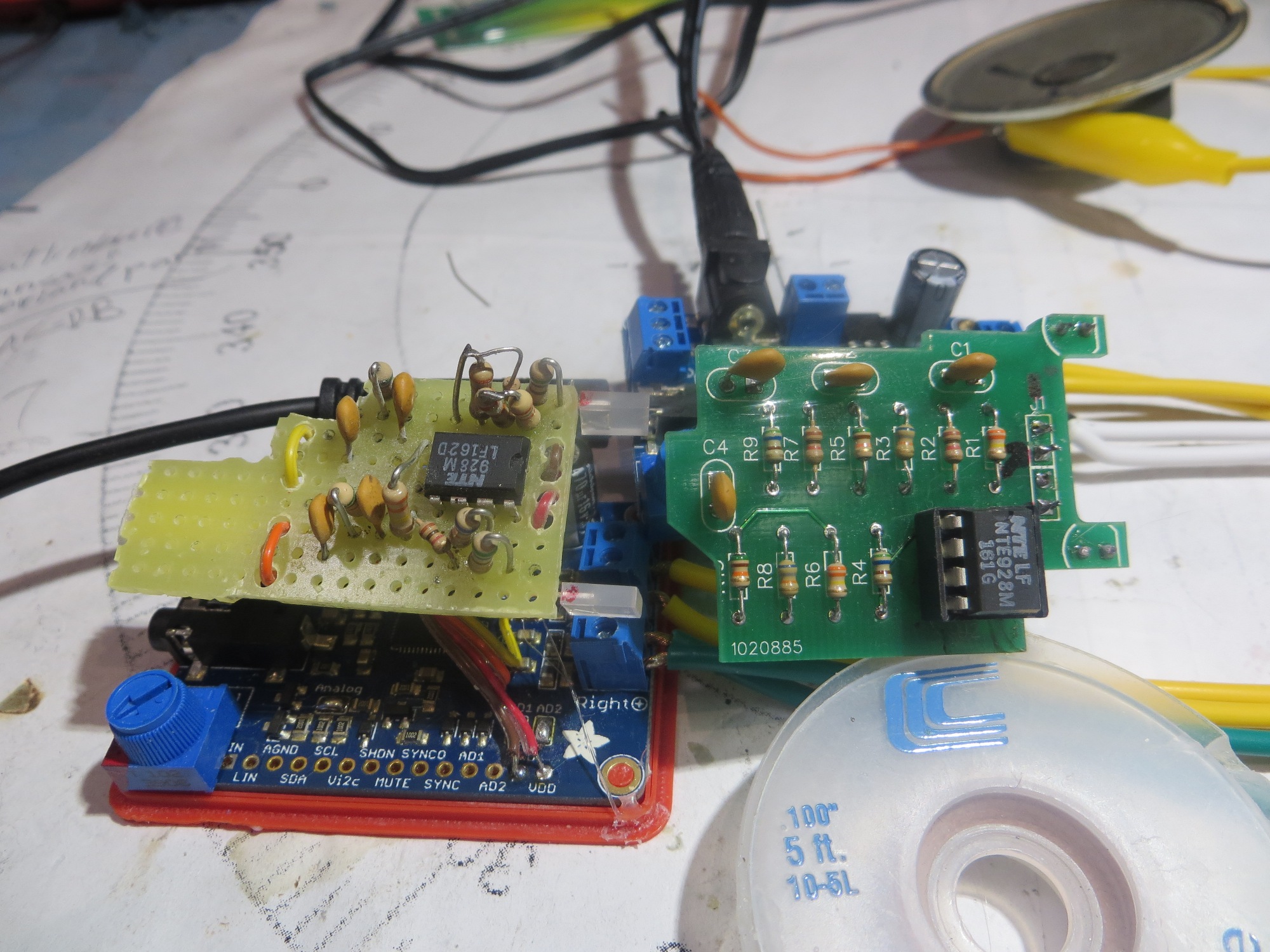
Completed PCB connected to Adafruit amplifier
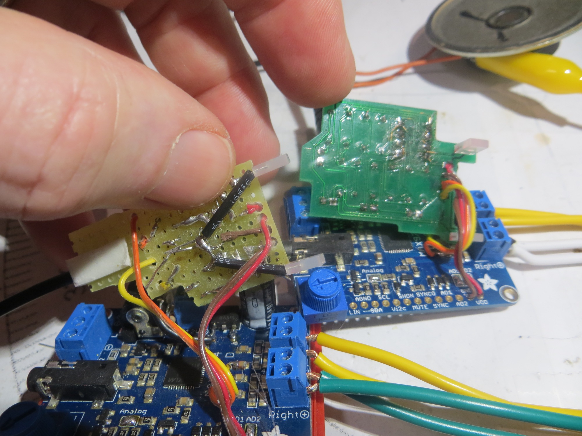
Bottom of PCB and hand-wired original (note messy area around op-amp)
The last thing to do was to get the PCB actually mounted onto the amplifier board, and the assembly into its custom-printed housing, as shown in the following images.
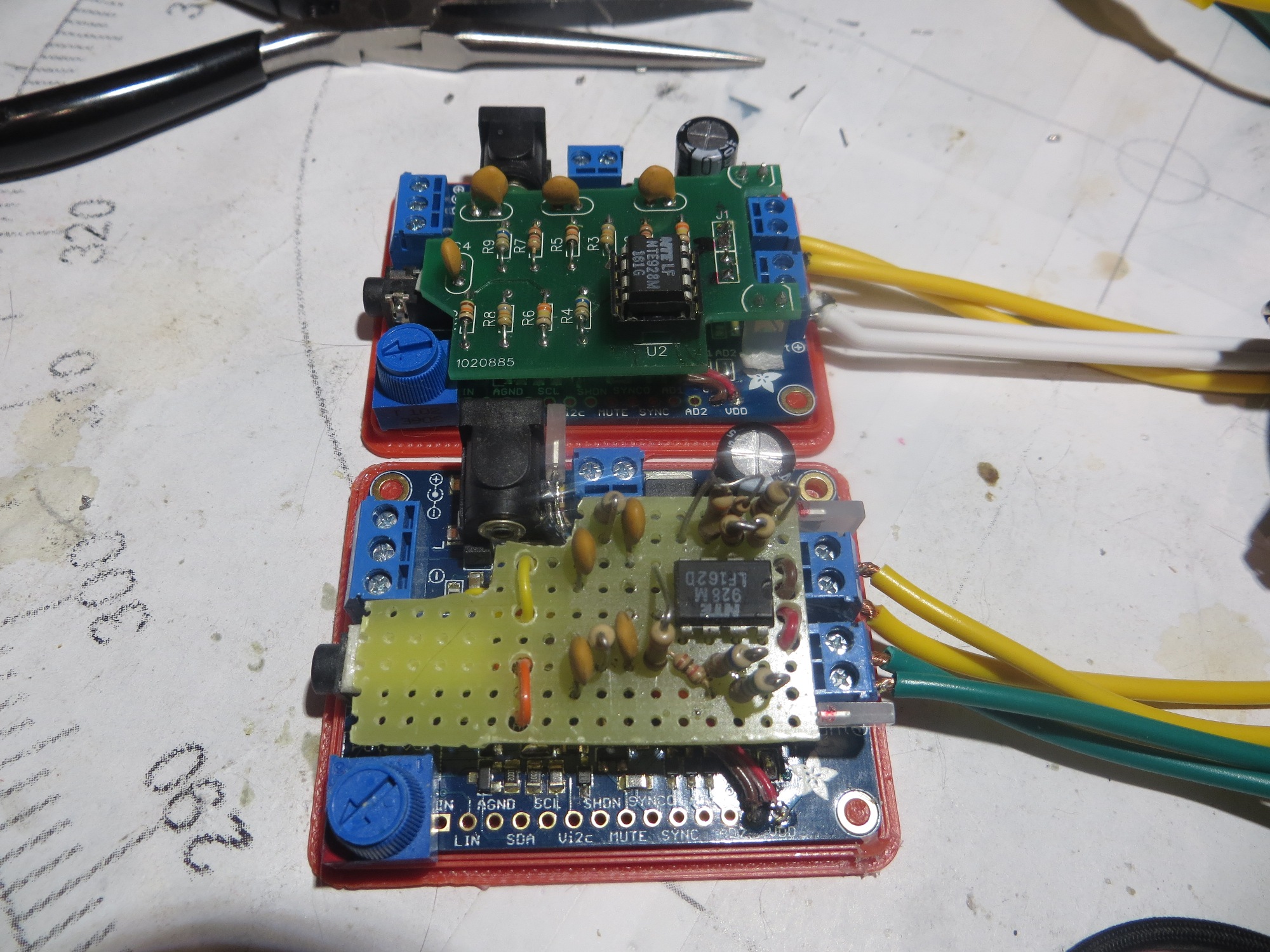
hand-wired and Rev2 PCB mounted to the Adafruit amp boards
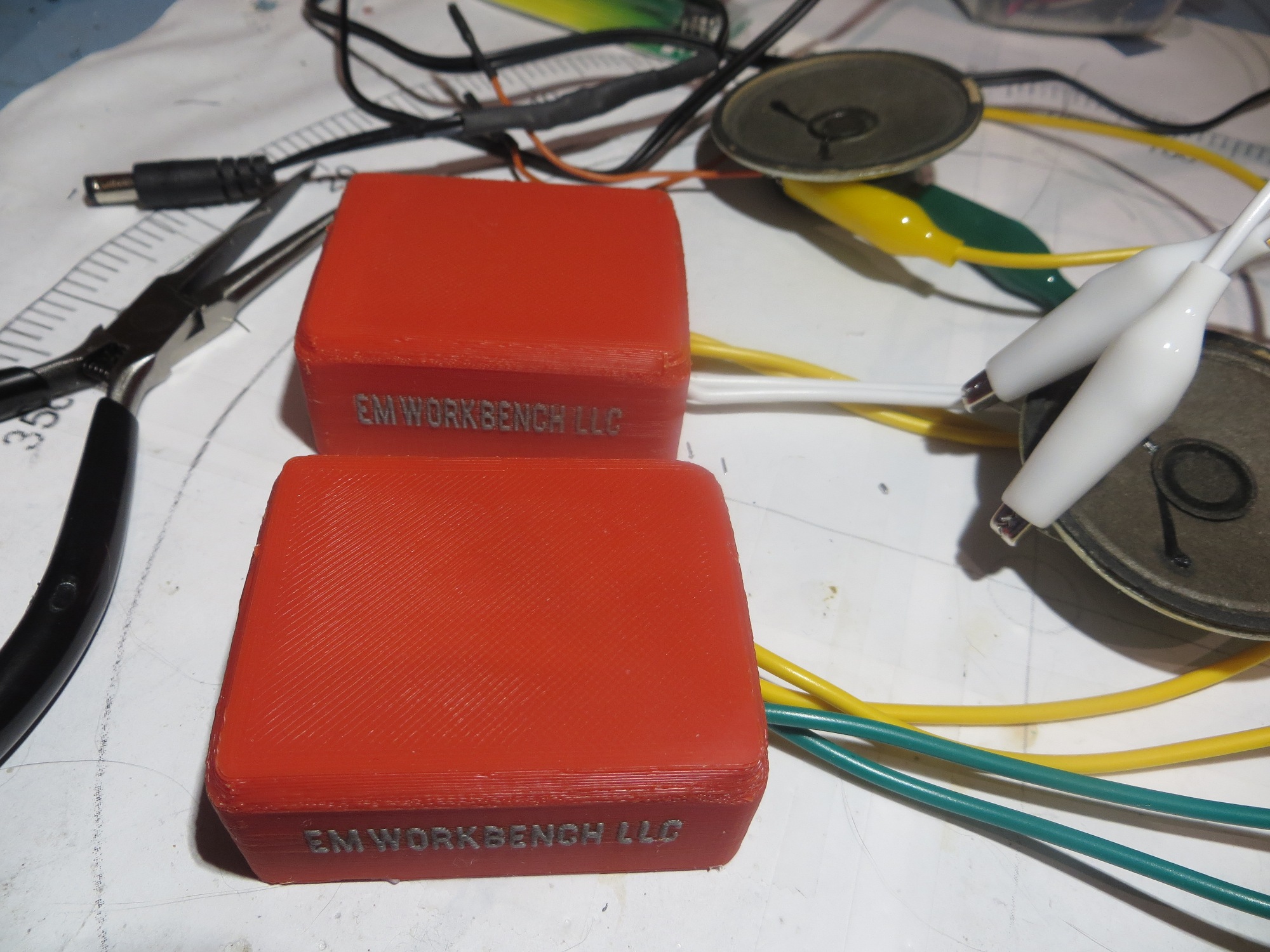
hand-wired and rev2 PCB mounted in custom-printed enclosures.
Now all I need is a ‘speaker’ presentation so I can find out if all this work was really worthwhile (actually, I’ve already had a great time with this project, so having it actually work for the students will just be icing on the cake!)
Pingback: Speaker Amplifier Project, Part VI - Second Production Run - Paynter's Palace