
Posted 05/14/17
In a previous post, I mentioned that John Jenkins, mentor and old friend, had some ideas regarding my Wall-E2 robot’s problems with homing in on an IR beam in the presence of ambient IR sources like overhead incandescent lighting and/or sunlight streaming in through windows and doors. John pointed out that this was really a system dynamic range issue, and it was likely that, as currently configured, the IR phototransistors were running out of dynamic range (saturating) well before the 10-bit A/D’s on the AtMega SBC. In order to get the detector sensitivity up to the point where Wall-E2 could ‘see’ the IR beam far enough (1.5-2m) away to avoid hanging up on the lead-in rails (see this post and this post for details), I had to use a very high value collector resistor (330K), which reduces the dynamic range significantly.
In a subsequent email conversation, John suggested that the proper way to handle this problem was to reduce the collector resistor to the point where the detector doesn’t saturate under the worst case ambient IR conditions, and then add amplification as necessary after the detector stage to get the required sensitivity. John’s point was that as long as the detector response is relatively linear (i.e., it’s not saturated), then there shouldn’t be any loss of information through the stage, so a later linear amplification stage will allow the desired IR signal to be detected/processed even in the presence of interference. However, if the detector stage saturates due to interference, then it’s basically ‘game-over’ in terms of the ability to later pull the desired signal out of the noise.
This wasn’t exactly what I wanted to hear, as adding the required post-detector amplification stage wasn’t going to be particularly easy – there’s not much left in the way of free real-estate on Wall-E2’s main platform (there’s plenty of room on the second level, but putting stuff there requires inter-level cabling and is a major PITA). As I was thinking this, I had a flashback to similar conversations with John from 40-45 years ago, when we were both design engineers in a USG design lab; the usual outcome of such ‘conversations’ (to the uninitiated these might be mistaken for shouting matches) was that my circuit got ‘simplified’ by the addition of 50% more parts – but could then withstand a nuclear attack in the middle of a snowstorm at the South Pole!
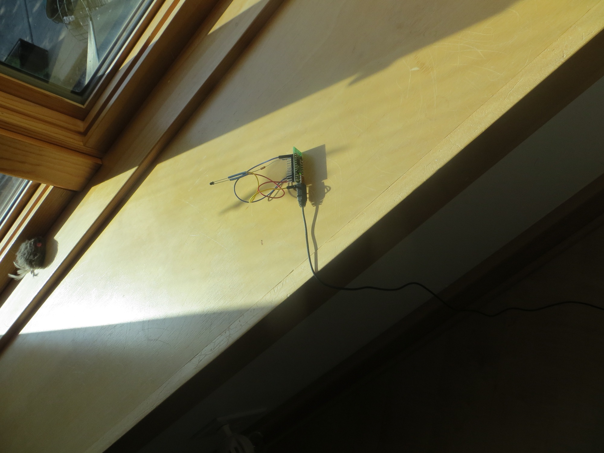
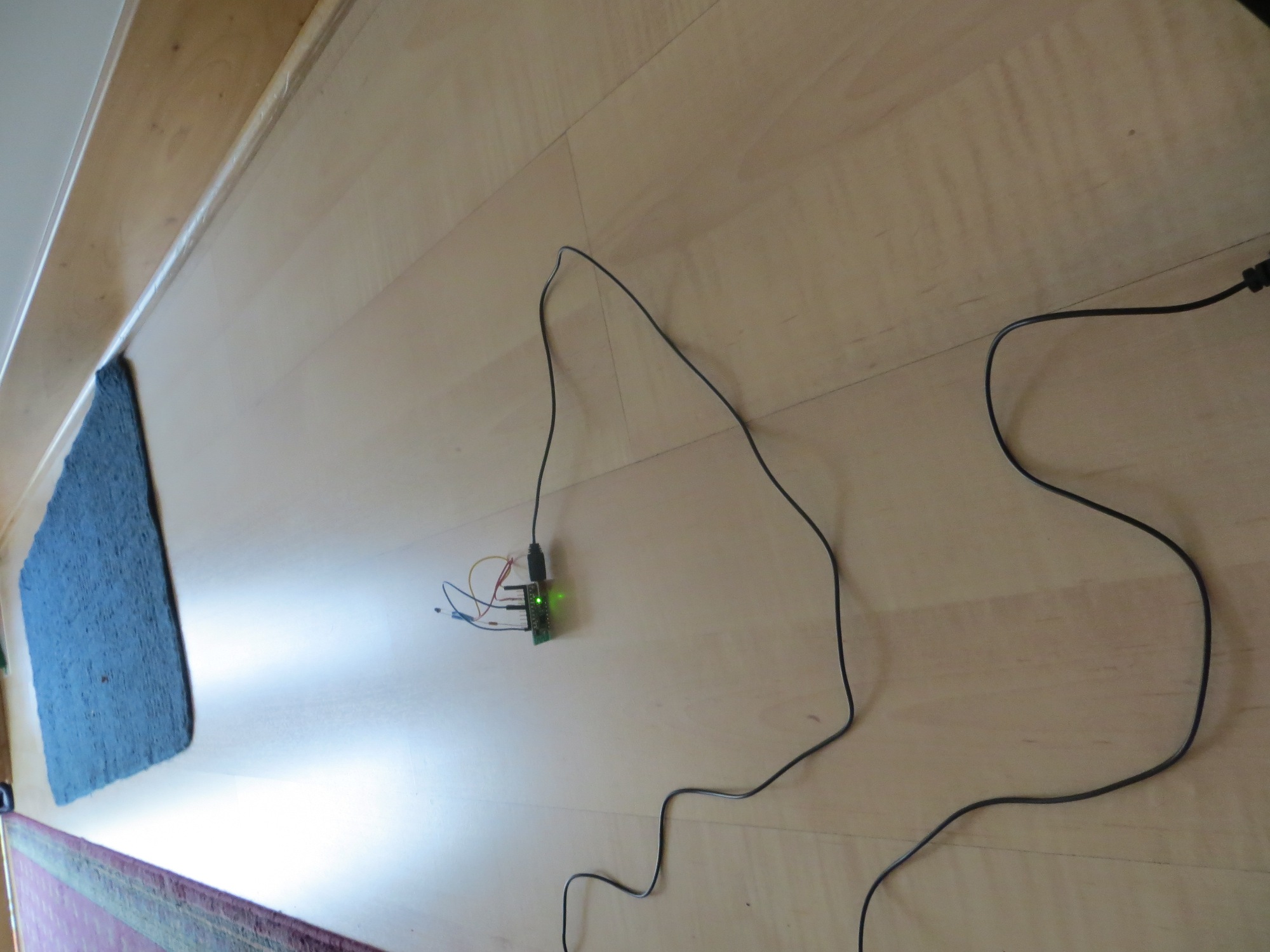
Anyway, back in the present, John suggested I run some experiments designed to determine the ratio of IR field intensity to collector current for a the phototransistors I was using, so the proper collector resistor value to be computed to utilize the available detector dynamic range without driving it into saturation. His suggestion was to not use a collector resistor at all, but to simply connect the collector to +VDC through a current meter, and then expose the detector to worst-case ambient conditions. I didn’t particularly like this idea, because I only have a manual non-recording multimeter, and I wanted to record the data for later analysis. So, I decided to program up one of my small SBC’s with analog input capability (in this case, a Pololu Wixel), and set up to measure the voltage drop across a 10 Ω precision resistor in the collector circuit. The hardware setup is shown in the following photo
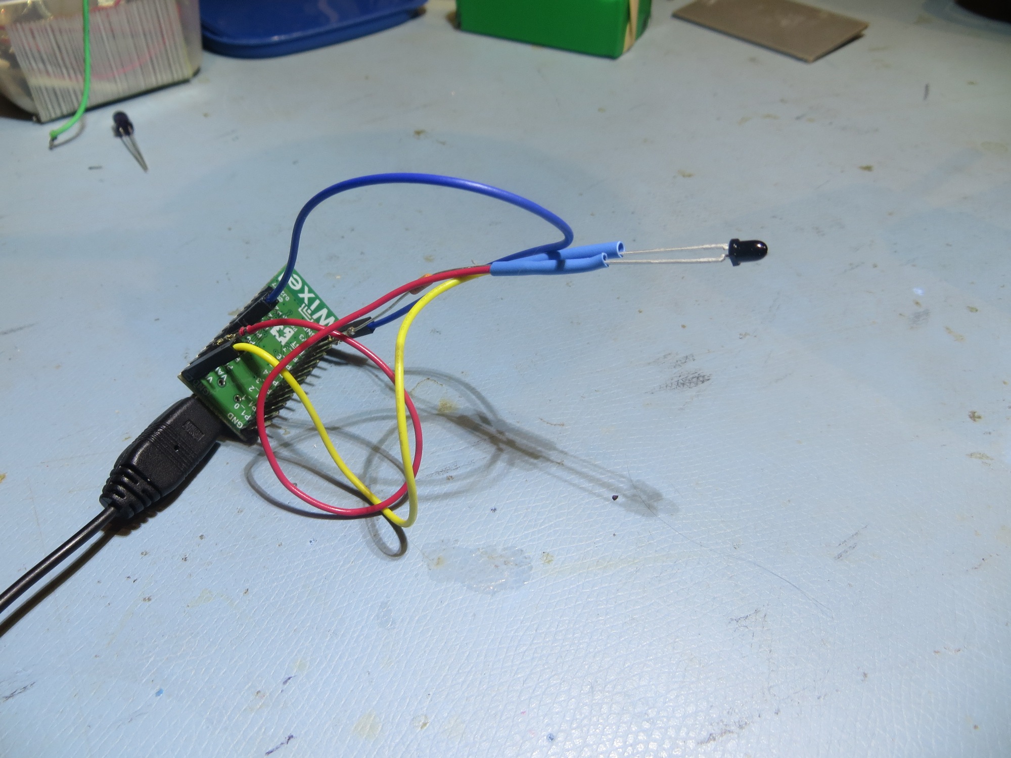
Hardware setup for IR Phototransistor Response Experiment
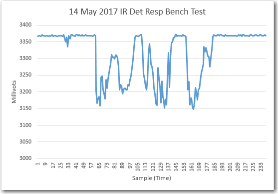
Before and after collecting ‘field’ data, I made a collection run on the bench, using my IR LED test box, with the following results. As can be seen in the plot, the maximum voltage drop across the 10Ω resistor was approximately 200mV, or about 20mA.
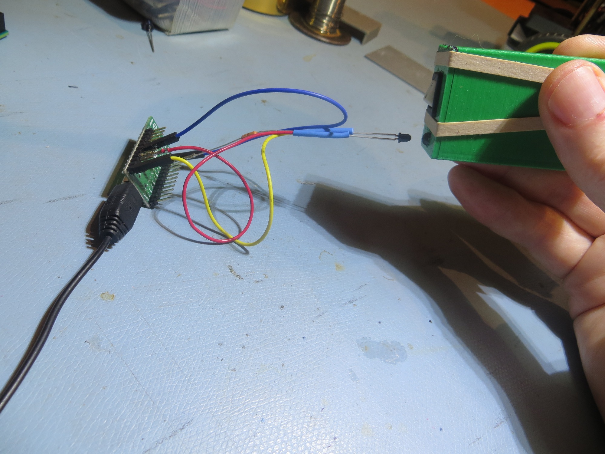
IR detector response bench test. Nose-to-nose with my IR test source
Bench test with IR LED test generator
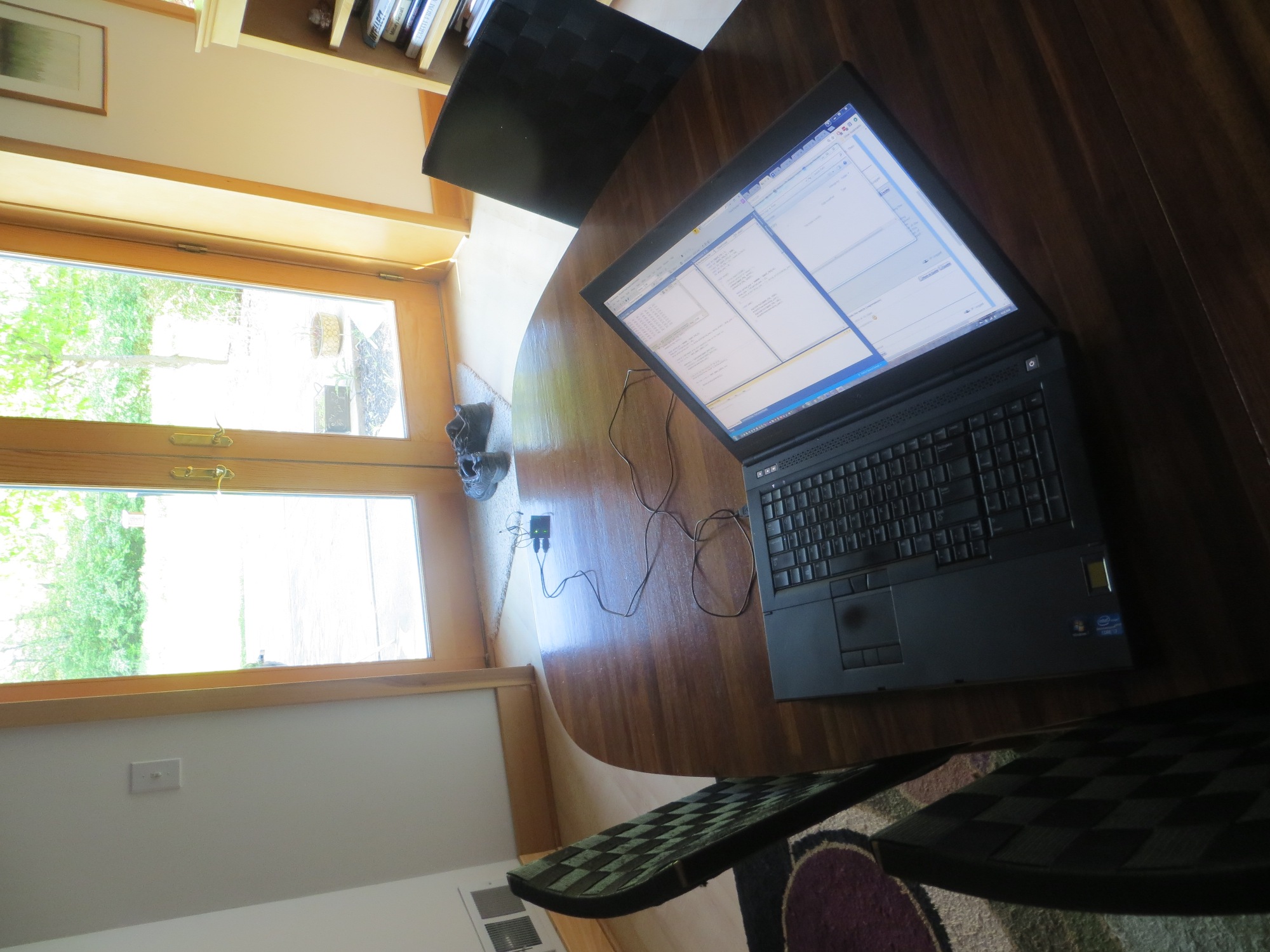
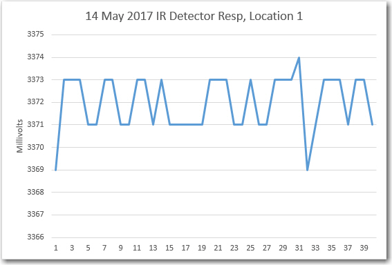
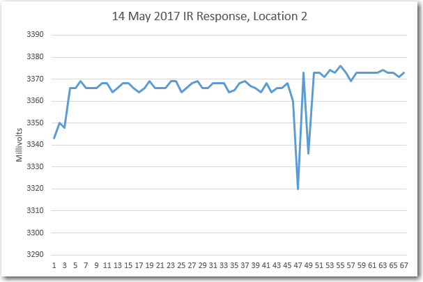
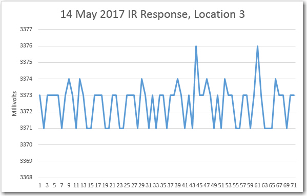
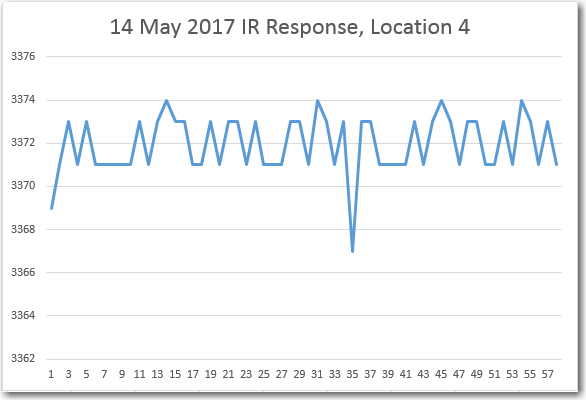
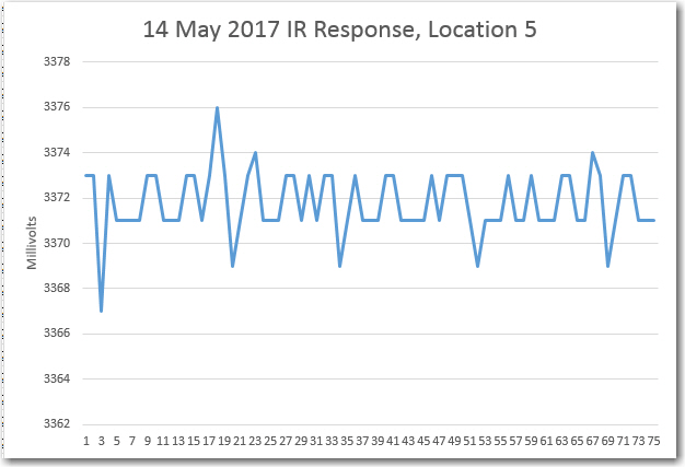
To collect the ‘field’ data, I placed the SBC in different locations around the house, and recorded A/D values. For these experiments I was using an example Wixel app that printed out the A/D values for all 6 analog inputs, scaled such that the maximum reading was equivalent to the SBC board voltage (3.3V) in millivolts. In other words, the maximum A/D reading was approximately 3375, or about 3 mV/bit
Location 1: Looking out glass doors on south side of house
Location 2: Direct sunlight through window on south side of house
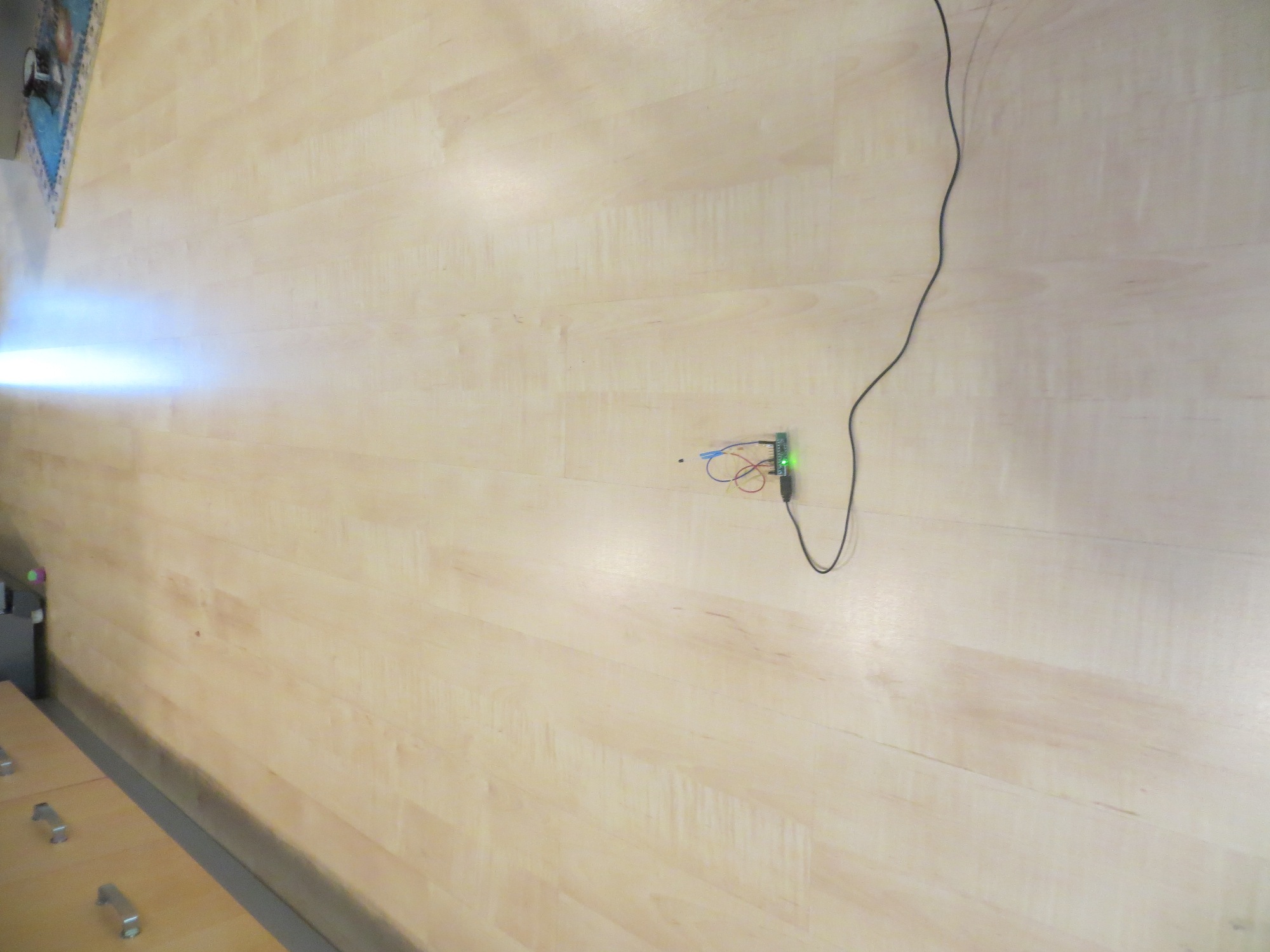
Location 3: Kitchen floor, looking toward entrance hall and atrium
Location 4: Entry hallway, looking toward atrium. This is the usual starting location for charging station homing tests
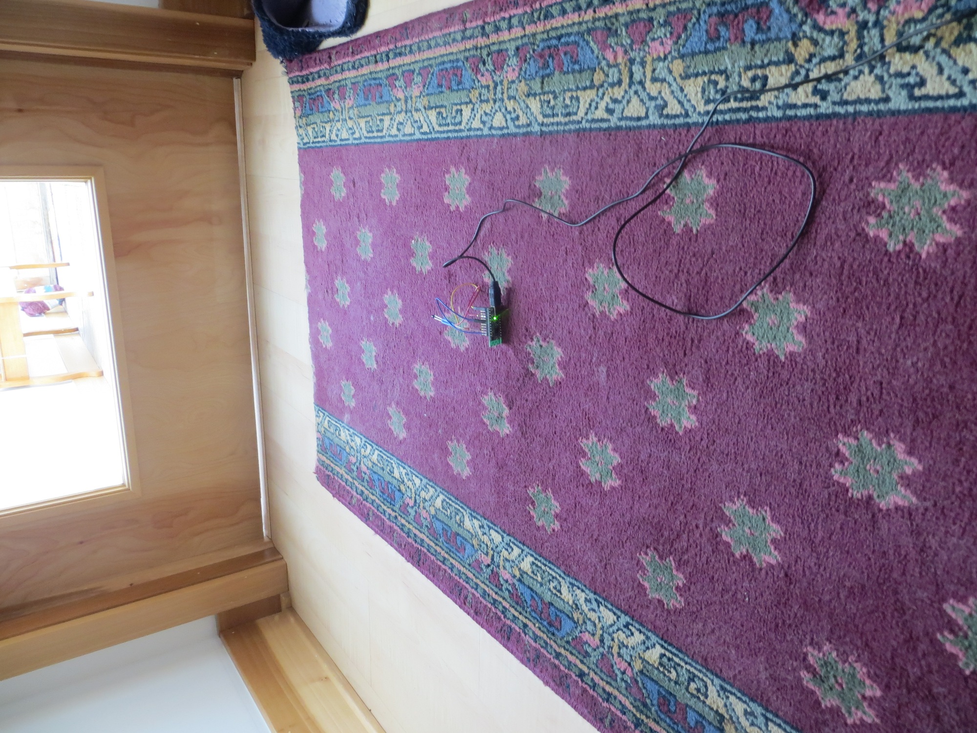
Location 5: Entry hallway near door to atrium
These results were not at all what I expected. Either there is something wrong with the experimental setup, or the ambient light IR field intensity isn’t anywhere near as strong as expected. If the data can be believed, the ambient conditions are significantly weaker than the bench-test conditions, which were basically nose-to-nose with my IR test LED. So, if my planned double-check of the hardware doesn’t find any problems, then I’ll change the resistor value from 10Ω to 100Ω and repeat the tests.
17 May 2017 Update
After thoroughly reviewing the hardware setup, I concluded that everything was working properly, but that the 10Ω load resistor simply didn’t provide sufficient drop for reliable measurements. So, I changed out the 10Ω resistor for 100Ω, and repeated the tests, with the following changes:
- As before, I started the run by performing a ‘nose-to-nose’ test to verify proper operation, but this time I measured the detector current using a multimeter. The result was about 15mA maximum current.
- At each of the 5 locations, I started with a short nose-to-nose section (not shown in the plots) to make sure the detector was operating properly
- At location 2 (the direct sunlight location), I physically oriented the detector for maximum response.
- After location 5, I placed the detector on the charging station’s IR beam reflector boresight at about 0.5m distance, and physically oriented the detector for max response.
- I calculated the detector current for each reading, and plotted that rather than the raw reading. To calculate the detector current for each measurement, I subtracted the detector reading from the corresponding 3.3VDC supply voltage measurement and divided by 100.
The results of these tests are shown in the plots below:
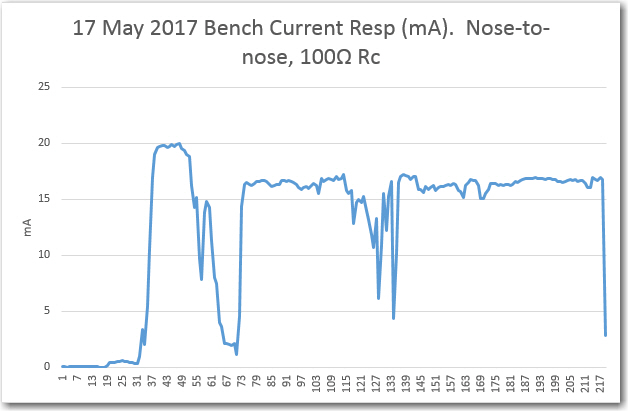
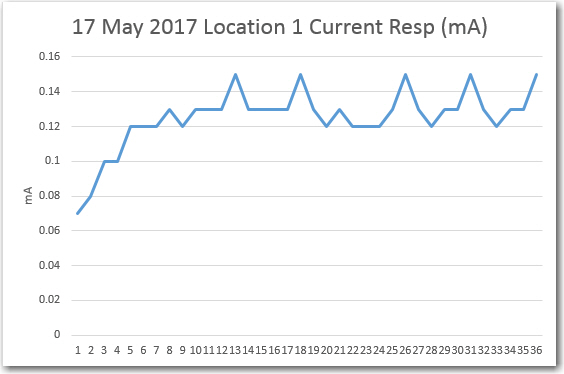
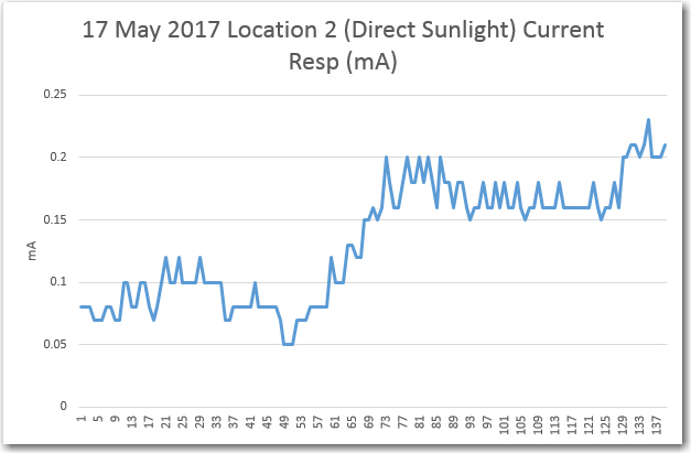
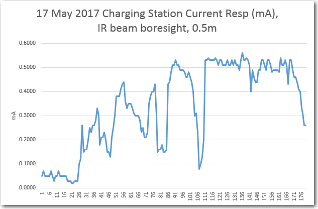
These results are pretty interesting. As I’m sure John would point out, the direct sunlight response of about 0.2 mA is about 20 times the value required to saturate the phototransistor with the current 330KΩ. No wonder I was having interference problems – oops!
Stay tuned!
Frank
Pingback: IR Homing Module Integration, Part IV - Paynter's Palace